Light-emitting diode

A technology of light-emitting diodes and electrodes, applied in electrical components, circuits, semiconductor devices, etc., can solve the problems of reduced luminous efficiency, influence of luminous efficiency of components, loss of light, etc., and achieve the effect of improving luminous efficiency

Inactive Publication Date: 2011-01-12
UBILUX OPTOELECTRONICS CORP
View PDF1 Cites 6 Cited by
  • Summary
  • Abstract
  • Description
  • Claims
  • Application Information

AI Technical Summary

Problems solved by technology

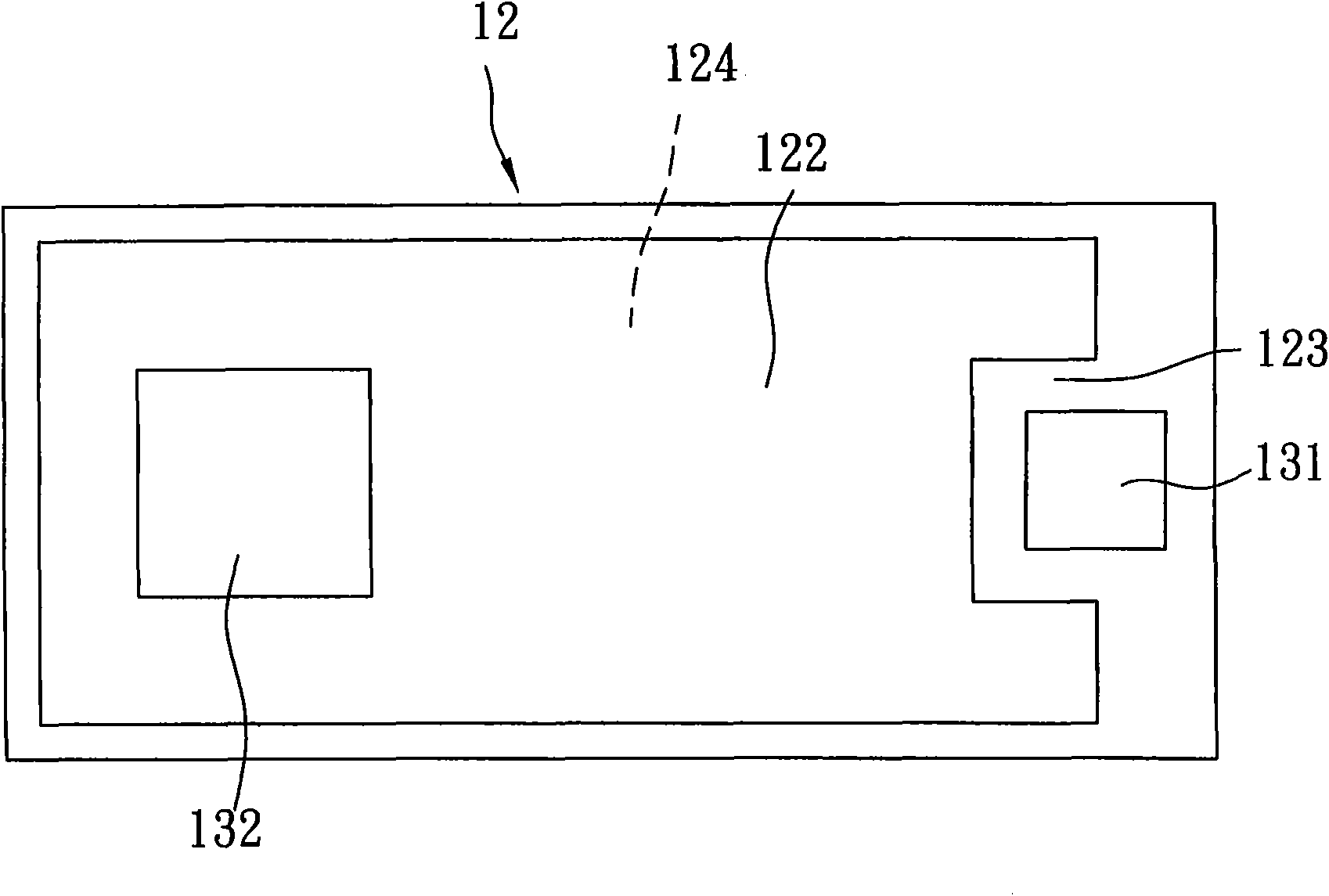
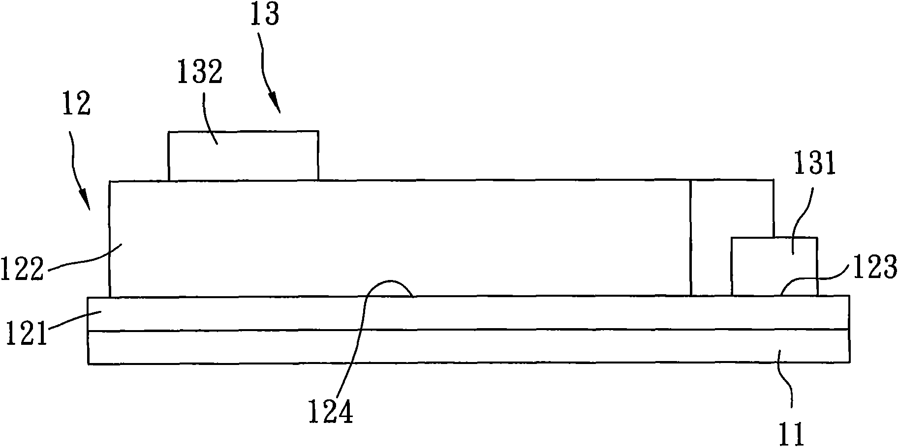
[0004] For the current horizontal light-emitting diodes, although it is true that they can emit light when electric energy is supplied, because the first electrode 131 and the second electrode 132 are opaque, they will be affected by the first electrode 131 and the second electrode 132 when generating light energy. The shielding of the second electrode 132 loses most of the amount of light emitted outwards, and when the first electrode 131 and the second electrode 132 cooperate to provide electric energy to the action film 12, it is also easy to be caused by the first electrode 131 and the second electrode 132. The shape of the second electrode 132 is a simple rectangular design, so that the uniformity of current injection is not good, and the luminous efficiency of the device is also affected at the same time.
[0005] In order to improve the problem of the reduction of luminous efficiency caused by the structure of the electrode, many methods for improving the structure of the electrode have been proposed one after another.

Method used

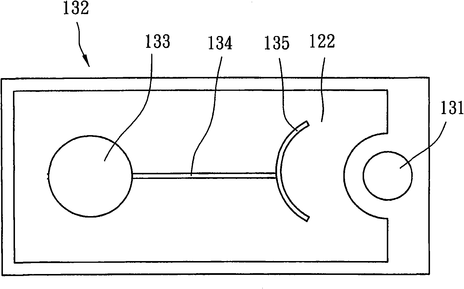

Image

  • Light-emitting diode
  • Light-emitting diode
  • Light-emitting diode

Examples


Embodiment Construction

[0029] The present invention will be described in detail below in conjunction with the accompanying drawings and embodiments.

[0030] refer to Figure 7 , Figure 8 , Figure 8 is selected from Figure 7 In the cross-sectional view of line 8-8, a preferred embodiment of the high-brightness light-emitting diode of the present invention includes a substrate 2, an action film 3 formed on the substrate, and an electrode unit 4. The electrode unit 4 can cooperate to provide The electric energy is sent to the action film 3, and the action film 3 can convert the electric energy into light energy by the photoelectric effect after receiving the electric energy and then send it out.

[0031] The substrate 2 is made of an insulating material. Since the constituent materials of the substrate 2 are well known to those skilled in the art, no more details are given here. In this embodiment, the substrate 2 is rectangular and made of sapphire. constituted, and define a direction perpendi...


PUM


Abstract

The invention provides a light-emitting diode comprising a base material, an action membrane and an electrode unit; particularly, the action membrane comprises a bottom connected with the base material and a platform part extending upwards from the bottom; the bottom comprises an opening region, a middle region, a first region and a second region, wherein, the middle region extends towards the first direction from the opening region; the first region and the second region are positioned at the two sides opposite to the opening region and the middle region; the electrode unit comprises a firstelectrode and a second electrode, wherein, the first electrode is arranged on the opening region; the second electrode is arranged on the top surface of the platform part; the width specific value ofthe first region and the second region which are vertical to the first direction is between 0.6 to 0.95; and the light-emitting efficiency of the light-emitting diode can be effectively promoted by utilizing the specific setting of the width specific value of the first region and the second region which are vertical to the first direction.

Description

technical field [0001] The invention relates to a light-emitting diode, in particular to a high-brightness light-emitting diode. Background technique [0002] refer to figure 1 , figure 2 , the current horizontal light emitting diode (Light EmittingDiode; LED) includes a rectangular substrate 11, an action film 12 and an electrode unit 13, the substrate 11 is made of sapphire, and the action film 12 accepts the electrode unit 13 When the electric energy is provided, it can emit light by photoelectric effect. It includes a bottom 121 connected to the base material 11 and a platform 122 extending upward from the bottom 121. The bottom 121 has a short side extending from one short side to the other. An open area 123 that extends in the short side direction and is square and an outer area 124 that contains the open area 123, and the platform 122 is integrally formed upward from the outer area 124; structurally, the action film 12 has a An n-type semiconductor layer connected...

Claims


Application Information

Patent Timeline
Patent Type & Authority Applications(China)
IPC IPC(8): H01L33/00
Inventor 林志胜吴哲雄
Owner UBILUX OPTOELECTRONICS CORP
Why Eureka
Try Eureka