Parasitic transversal NPN component and manufacturing method

A lateral device technology, applied in the manufacture of parasitic lateral NPN devices, in the field of parasitic lateral NPN devices, can solve the problems of large area, weak current capability, small gain, etc., achieve uniform diffusion distribution, improve current capability, and improve Effect of Cutoff Frequency

Active Publication Date: 2013-06-05
SHANGHAI HUAHONG GRACE SEMICON MFG CORP
View PDF5 Cites 0 Cited by
  • Summary
  • Abstract
  • Description
  • Claims
  • Application Information

AI Technical Summary

Problems solved by technology

The disadvantage of the existing LNPN device is that the area is large, and the current in the base area is an L-shaped structure, the current capability is weak, and the gain is small

Method used


Image

  • Parasitic transversal NPN component and manufacturing method
  • Parasitic transversal NPN component and manufacturing method
  • Parasitic transversal NPN component and manufacturing method

Examples


Embodiment Construction

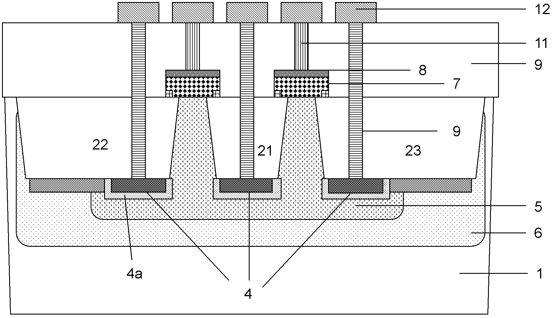
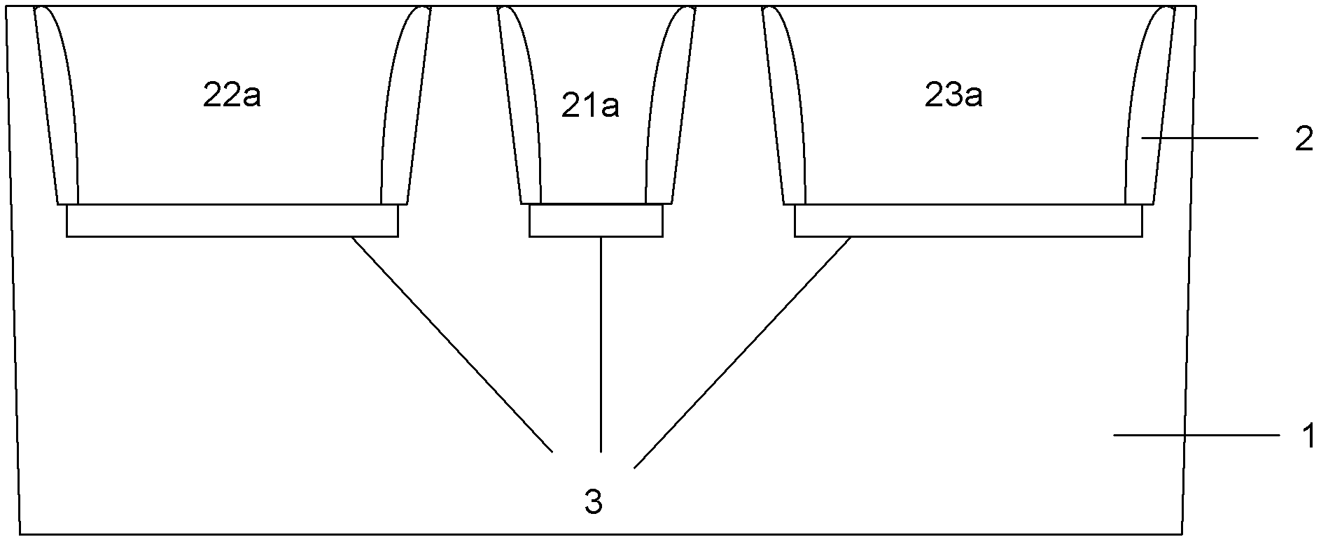
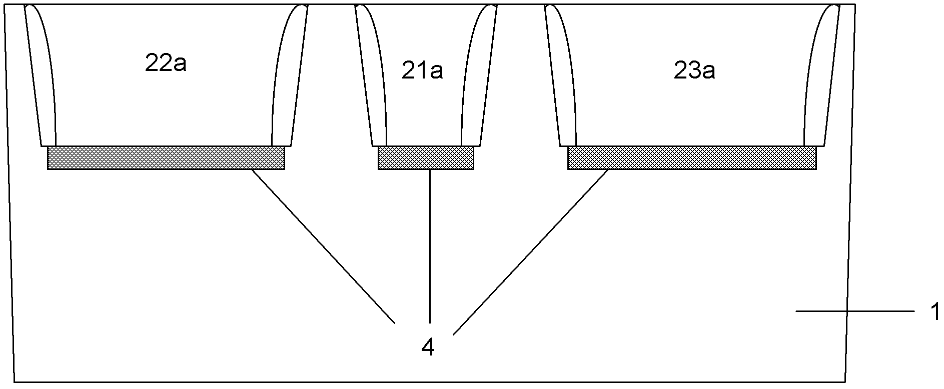
[0040] Such as figure 2 Shown is a schematic diagram of the structure of a parasitic lateral NPN device according to an embodiment of the present invention. In the embodiment of the present invention, a parasitic lateral NPN device is formed on a P-type silicon substrate 1, and the active region is isolated by shallow trench field oxygen, that is, the isolation structure of the active region is shallow trench isolation (STI), and the shallow trench field oxygen The depth is 0.3 micron to 0.5 micron. Parasitic lateral NPN devices include:

[0041] A base region 5 is composed of P-type injection layers formed in two adjacent first active regions and second active regions. The P-type injection layer can share the P- injection layer in the vertical PNP (VPNP) in the bipolar device (Bipolar) process, or share the P-type well process in the BiCMOS process. The implant dose of the P-type ion implantation of the P-type implant layer is 1e12cm -2 ~5e13cm -2 , the implantation ene...


PUM


Abstract

The invention discloses a parasitic transversal NPN component. A base region is formed by P-shaped injection layers formed in two adjacent active areas, an emitter region is formed by N-shaped mixed polycrystalline silicon buried layers formed on the bottom of shallow groove oxygen between the two active regions of the base region, and a current collection region is formed by the N-shaped mixed polycrystalline silicon buried layers formed on the bottom of the shallow groove oxygen on two sides of the two active regions of the base region. The structure of the component is C-B-E-B-C. The structure can enable a current path in the base region of the component to change into a linear shape, improve current capacity of the component, and enable current gain and frequency characteristic of the component to be improved greatly, reduce area of the component and provide current density. The polycrystalline silicon buried layers can reduce connecting resistance of an emitter and a collector, enable the resistance to be uniform, and greatly improve cut-off frequency of the component. The invention further discloses a manufacturing method of the parasitic transversal NPN component.

Description

technical field [0001] The invention relates to the field of manufacturing semiconductor integrated circuits, in particular to a parasitic lateral NPN device; the invention also relates to a manufacturing method of the parasitic lateral NPN device. Background technique [0002] In radio frequency applications, higher and higher device characteristic frequencies are required. Although RFCMOS can achieve higher frequencies in advanced process technologies, it is still difficult to fully meet radio frequency requirements. For example, it is difficult to achieve characteristic frequencies above 40GHz, and advanced technology The research and development cost of compound semiconductors is also very high; compound semiconductors can realize very high characteristic frequency devices, but due to the disadvantages of high material cost and small size, and the toxicity of most compound semiconductors, its application is limited. Silicon germanium (SiGe) heterojunction bipolar transis...

Claims


Application Information

Patent Timeline
Patent Type & Authority Applications(China)
IPC IPC(8): H01L29/08H01L29/10H01L29/04H01L29/417H01L29/735H01L21/28H01L21/331
Inventor 陈帆陈雄斌薛恺周克然潘嘉李昊蔡莹陈曦
Owner SHANGHAI HUAHONG GRACE SEMICON MFG CORP
Why Eureka
Try Eureka