

Photosensitive assembly
A technology of photosensitive components and gates, which is applied in the direction of electrical components, semiconductor devices, circuits, etc., to achieve the effect of improving photosensitive efficiency
Inactive Publication Date: 2011-01-26
CHUNGHWA PICTURE TUBES LTD
View PDF0 Cites 0 Cited by
- Summary
- Abstract
- Description
- Claims
- Application Information
AI Technical Summary
Problems solved by technology
However, even though the current ALS technology can directly integrate the function on the substrate of the liquid crystal display, saving the need for an additional independent brightness sensor, how can it sense the most appropriate ambient light source in a limited space to reduce cost pressure and space constraints? Limitations still need to be worked on
Method used
View moreImage
Smart ImageViewing Examples

Examples
Embodiment Construction
Login to View More PUM
 Abstract
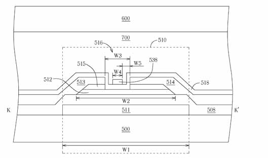
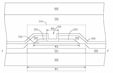
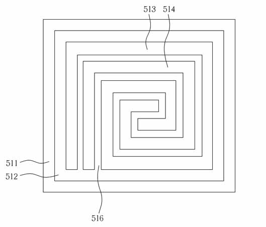
The invention relates to a photosensitive assembly, which is characterized by comprising a gate electrode, a gate electrode insulating layer, a semiconductor layer, a source electrode, a drain electrode and a channel part. The channel part is arranged between the source electrode and the drain electrode; the source electrode and the drain electrode are both arranged on the semiconductor layer, and are respectively provided with at least a first long comb electrode and at least a first short comb electrode as well as at least a second long comb electrode and at least a second short comb electrode; and the first long comb electrode and the first short comb electrode as well as the second long comb electrode and the second short comb electrode are arranged in an interlacing way by length. The invention can increase the area of a photosensitive region in the limited photosensitive assembly space so as to greatly promote the photosensitive efficiency, and thereby eliminating the current predicament in the industry.
Description
technical field The invention provides a photosensitive component, especially a photosensitive component arranged in a liquid crystal display for sensing ambient light sources. Background technique Liquid crystal displays are widely used in portable information devices such as notebook computers (notebooks) and personal digital assistants (personal digital assistants, PDAs) due to their thin and light appearance, low power consumption, and no radiation pollution. . Recently, as the functions of portable information devices become increasingly complex, the display quality requirements are increasing. How to display images clearly both indoors and outdoors has become an important issue in current liquid crystal display technology. Under such demands, technologies such as transflective mode liquid crystal display technology and ambient light sensor (Ambient Light Sensor, ALS) have emerged. Through ALS technology, the system can measure the intensity of ambient lighting a...
Claims
Login to View More Application Information
Patent Timeline
 Patent Type & Authority Applications(China)
IPC IPC(8): H01L31/10H01L31/0224H01L31/0352
Inventor 李威龙王文哲
Owner CHUNGHWA PICTURE TUBES LTD