
Printed circuit board lamination manufacturing process

A printed circuit and board pressing technology, which is applied in the field of printed circuit board lamination process technology, can solve the problems of increasing lamination time, increasing PP cutting and PP replacement times, and low pre-lamination efficiency, so as to reduce the interlayer Slip, reduce the number of PP cutting, improve the effect of production efficiency

Inactive Publication Date: 2011-02-02
昆山元茂电子科技有限公司
View PDF4 Cites 22 Cited by
  • Summary
  • Abstract
  • Description
  • Claims
  • Application Information

AI Technical Summary

Problems solved by technology

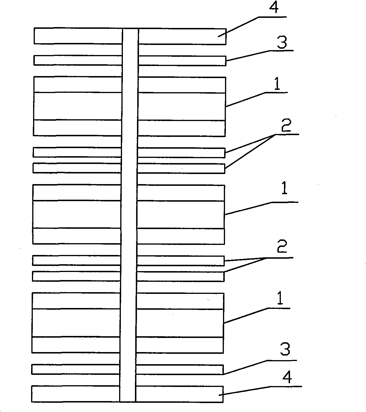
During the lamination process, when the staff stacks different types of PP, the parts are more complicated, which increases the lamination time and the pre-lamination efficiency is low; moreover, slippage easily occurs between the laminates, which increases the PP cutting and The number of PP replacements is time-consuming and labor-intensive, which affects production efficiency

Method used


Image

  • Printed circuit board lamination manufacturing process
  • Printed circuit board lamination manufacturing process
  • Printed circuit board lamination manufacturing process

Examples


Embodiment Construction

[0018] In order to make the technical means, creative features, goals and effects achieved by the present invention easy to understand, the present invention will be further described below in conjunction with specific embodiments.

[0019] This example:

[0020] This embodiment provides a printed circuit board lamination process, which includes the following steps:

[0021] (1), PP cutting: cut the PP of the same model into several small sheets through the PP slitting machine, and then use the cutting machine to cut it into the size required by the work order, and match it with the inner layer board;

[0022] There is only one type of PP in the PP layer in the new stack, which is more convenient to cut; while in the old stack, the inner layer contains two types of PP, and the PP model needs to be replaced when cutting the original stacked PP, and the replacement process takes about 15 to 20 minutes.

[0023] (2) Front pre-stacking: stack the inner layer board and the cut OK ...


PUM


Abstract

The invention discloses a printed circuit board lamination manufacturing process. The process is characterized by comprising the following steps of: (1) PP cutting; (2) pre-stacking in advance; (3) riveting; and (4) pre-stacking subsequently. In the process, by the steps, an intermediate film stacked structure of an eight-layer plate or a ten-layer plate in lamination operation adopts two films in the same model number and work staff is more accustomed to stacking the PP in the same model number, so that PP cutting times are reduced and PP replacing time of 15 to 25 minutes can be saved once; pre-stacking efficiency can be improved by about 30 percent by stacking two layers of the PP of the same model number compared with stacking two layers of PP of different model numbers; interlayer slippage is reduced; and production efficiency is improved.

Description

technical field [0001] The invention relates to the technical field of printed circuit board manufacturing, in particular to a printed circuit board lamination process. Background technique [0002] Due to the rapid development of electronic technology, the continuous development of printed circuit technology has been promoted. Printed circuit board (Print Circuit board referred to as PCB board) develops through single-sided-double-sided-multilayer, and the proportion of multilayer boards is increasing year by year. The performance of multilayer boards is developing towards two extremes: high, fine, dense, thin, large and small. An important process in the manufacture of multilayer boards is lamination, and the control of lamination quality is becoming more and more important in the manufacture of multilayer boards. [0003] Existing manufacturing double-layer or multi-layer metal PCB board, it is to print circuit on the substrate by printing, produce circuit after chemica...

Claims


Application Information

Patent Timeline
Patent Type & Authority Applications(China)
IPC IPC(8): H05K3/46H05K3/00
Inventor 徐守杰韩业刚
Owner 昆山元茂电子科技有限公司
Learn More