Optical device and method of manufacturing the same

A technology of an optical device and a manufacturing method, applied in the directions of optics, optical components, installation, etc., can solve the problem of unimproved fluctuation of a lens accommodating portion, and achieve the effects of minimizing the reduction of throughput and suppressing fluctuations

Inactive Publication Date: 2011-03-30
SONY CORP
View PDF8 Cites 0 Cited by
  • Summary
  • Abstract
  • Description
  • Claims
  • Application Information

AI Technical Summary

Problems solved by technology

Therefore, when only the ultraviolet curable resin near the lower end of the lens housing is cured to temporarily fix the time required, the fluctuation of the lens housing is not improved.

Method used


Image

  • Optical device and method of manufacturing the same
  • Optical device and method of manufacturing the same
  • Optical device and method of manufacturing the same

Examples


Embodiment Construction

[0030] Preferred embodiments of the present invention will be described in detail below with reference to the accompanying drawings.

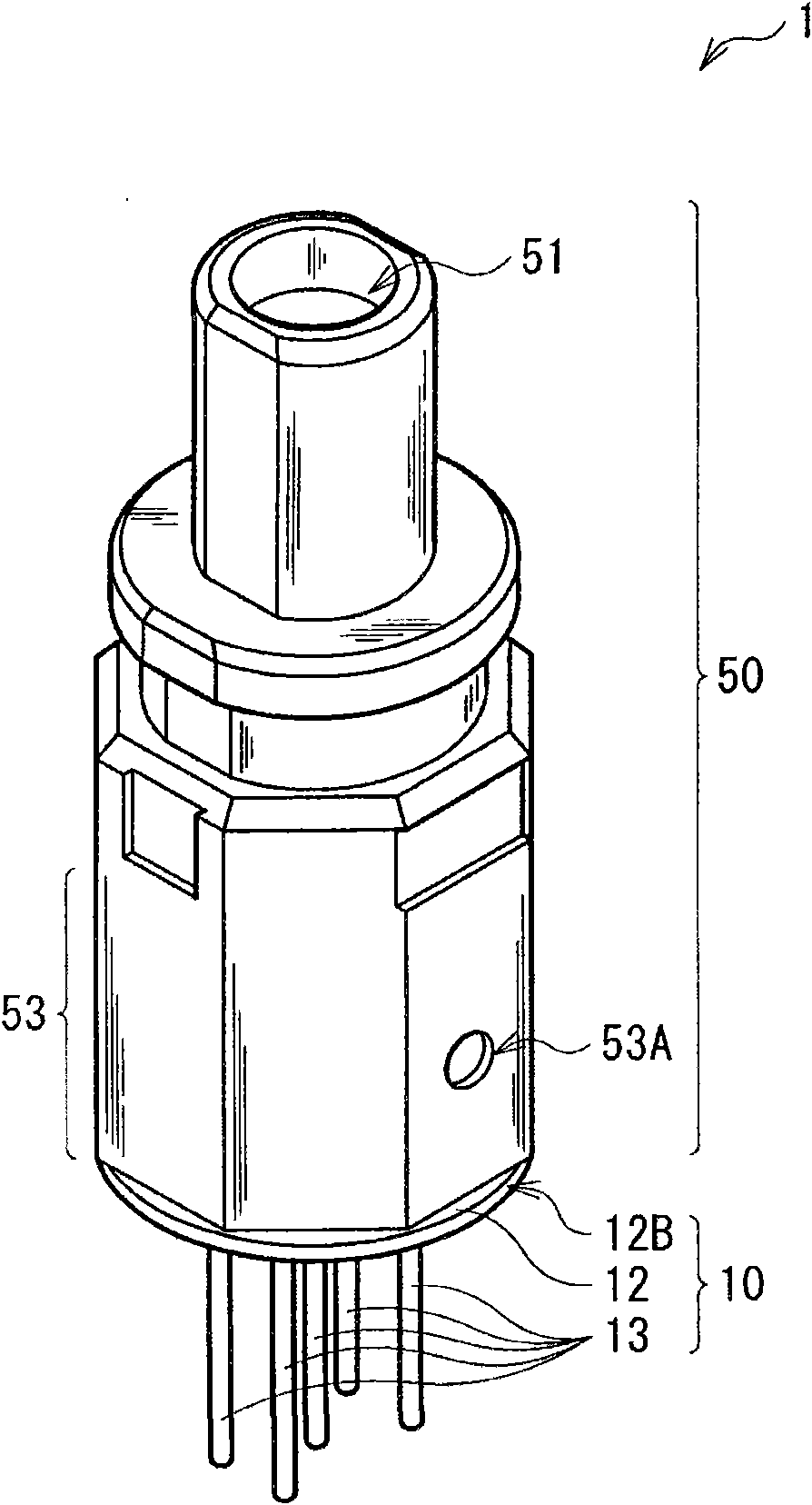
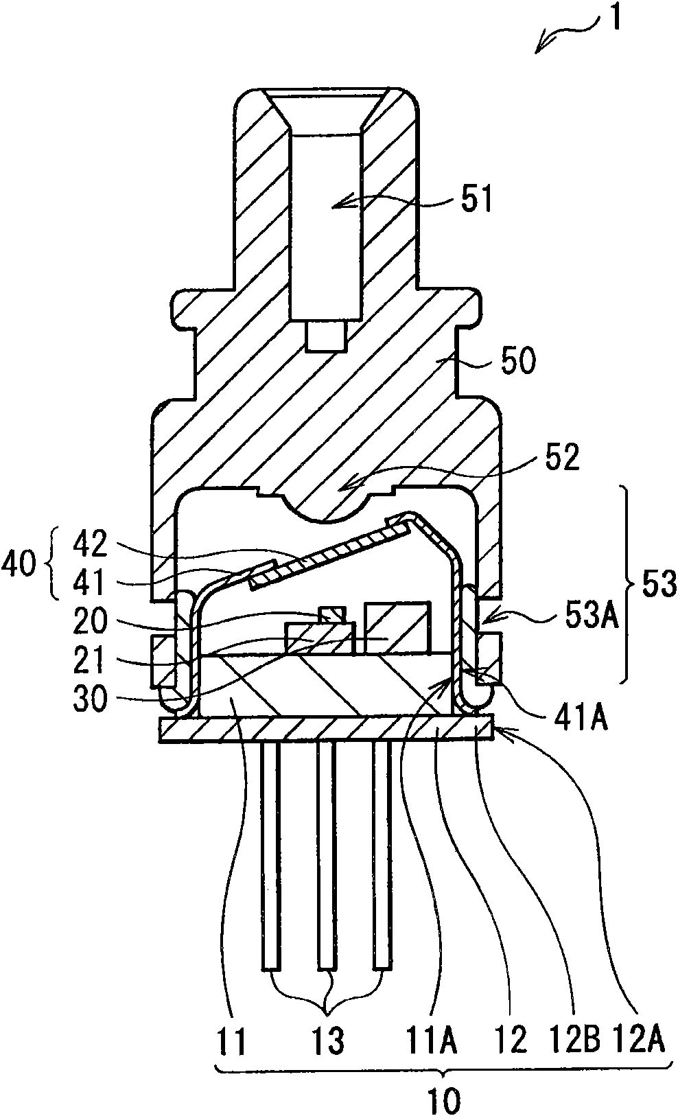
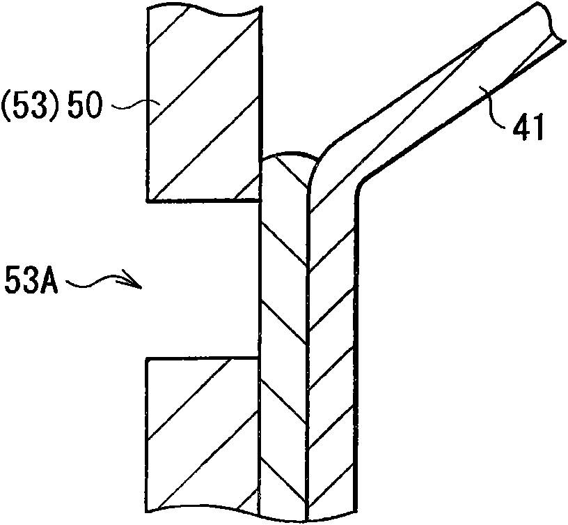
[0031] figure 1 It is a perspective view of a schematic structure of a light transmitter device (light transmitter device) 1 according to an embodiment of the present invention. figure 2 show figure 1 The cross-sectional structure of the optical transmitter. figure 1 and 2 are schematically shown configurations, and may differ from actual sizes or shapes.

[0032] The optical transmission device 1 of this embodiment is generally called TOSA (Transmitter Optical Sub Assembly, optical transmission sub-assembly), which converts an externally input electrical signal into an optical signal and outputs the optical signal. The light transmitting device 1 includes, for example, a stem 10 , a light emitting element 20 , a light receiving element 30 , a cap 40 and a lens housing 50 . The stem portion 10 corresponds to a specific example of the "bas...


PUM


Abstract

An optical device and a method of making an optical device is described herein. The optical device comprises a housing, an optical element, a base structure that supports the optical element and that interfaces with the housing to form a gap section between an outer wall section of the base structure and an inner wall section of the housing, a resin within the gap section fixing the housing to the base structure, and a light accommodation section in the housing. The light accommodation section accommodates a transmittance of light to the resin within the gap section.

Description

technical field [0001] The present invention relates to an optical device having a transmitting function of converting an electrical signal into an optical signal and outputting the optical signal, or a light receiving function of converting an optical signal into an electrical signal and outputting the electrical signal, and a manufacturing method thereof. Background technique [0002] In the XFP (10-Gibabit Small Form Factor Pluggable, 10Gb Small Form Factor Pluggable) module, which is the standard for optical receiving / transmitting modules, an optical device is installed, which includes an optical device that converts electrical signals into optical signals and outputs optical signals. A transmitting device, or a light receiving device that converts an optical signal into an electrical signal and outputs the electrical signal. In this optical device, for example, a light-emitting element or a light-receiving element is mounted on the top surface of a stem (stem) and seale...

Claims


Application Information

Patent Timeline
Patent Type & Authority Applications(China)
IPC IPC(8): G02B6/42
CPCG02B27/0916H01L31/0203G02B19/0061G02B19/0014G02B19/0095G02B6/4204G02B6/4239G02B6/4286G02B7/025
Inventor 成瀬晃和荒木田孝博中田英彦增井勇志城岸直辉
Owner SONY CORP
Why Eureka
Try Eureka