Display apparatus and method of manufacturing the same

Inactive Publication Date: 2008-12-18
CASIO COMPUTER CO LTD
View PDF36 Cites 45 Cited by
  • Summary
  • Abstract
  • Description
  • Claims
  • Application Information

AI Technical Summary

Benefits of technology

[0012]It is an object of the present invention to provide a display apparatus that has excellent display characteristics without any image blurring or t

Problems solved by technology

This causes an optical path difference corresponding to the film thickness between the applied light beams, which then causes chromaticity sh

Method used


Image

  • Display apparatus and method of manufacturing the same
  • Display apparatus and method of manufacturing the same
  • Display apparatus and method of manufacturing the same

Examples


first embodiment

[0076](Device Structure of Display Pixel)

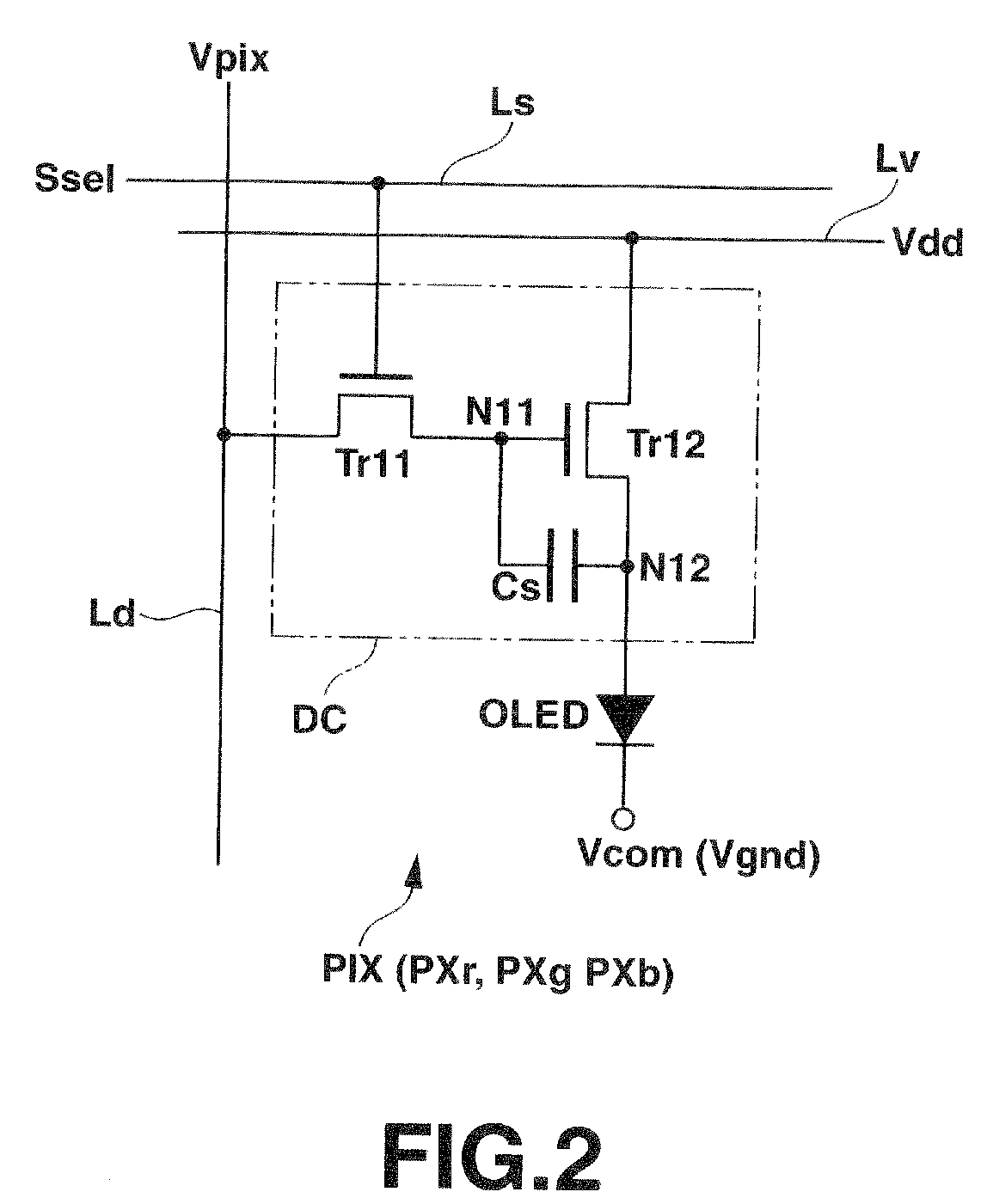
[0077]The device structure (plan layout and sectional structure) of a display pixel (a pixel driving circuit and an organic EL element) having the above circuit arrangement will be described in detail next.

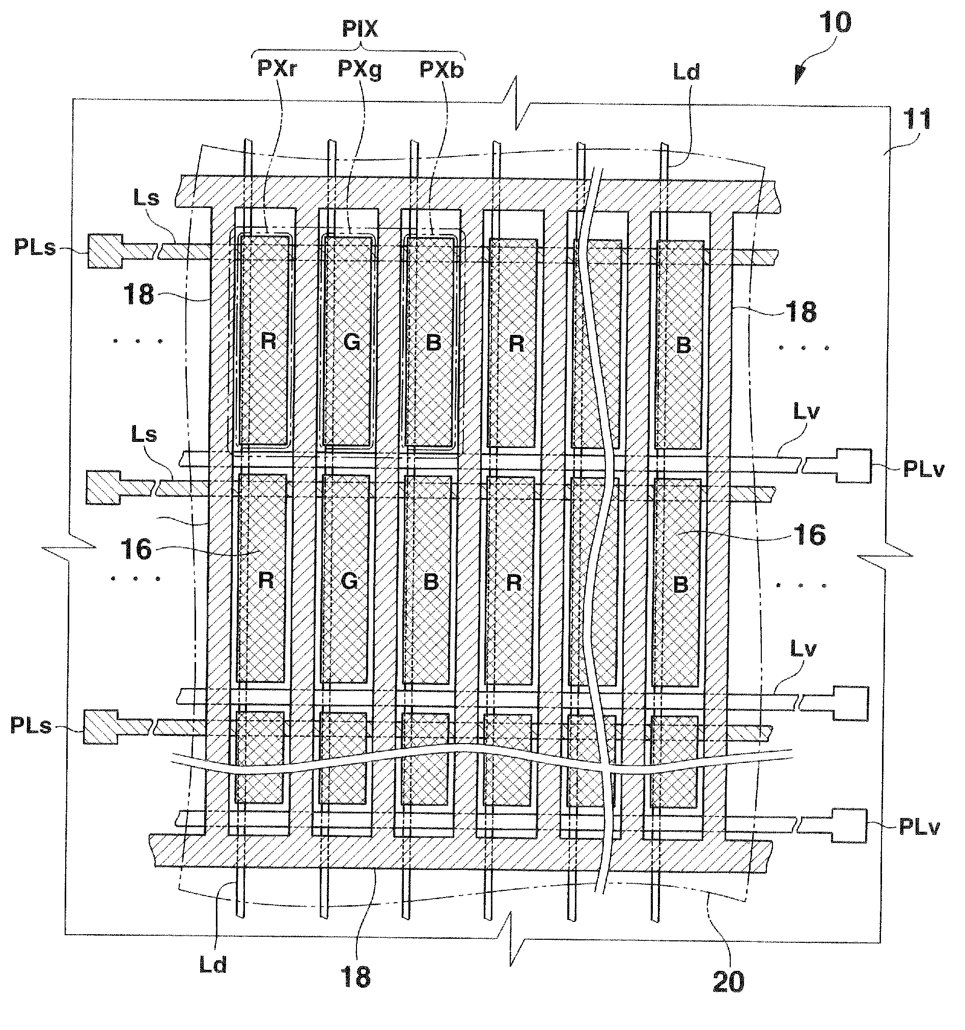
[0078]FIG. 3 is a plan layout showing an example of a display pixel that can be applied to a display apparatus (display panel) according to the first embodiment. FIG. 3 shows a plan layout of a specific one of color pixels PXr, PXg, and PXb of red (R), green (G), and blue (B) of a display pixel PIX shown in FIG. 1. Note that FIG. 3 mainly shows a layer on which the transistors, interconnection layers, and the like of a pixel driving circuit DC are formed. For the sake of convenience, the respective interconnection layers and the respective electrodes are hatched to clearly indicate their arrangement. FIGS. 4A, 4B, and 5 are schematic sectional views showing the A-A section and B-B section of the display pixel PIX having the plan layout show...

second embodiment

[0193](Device Structure of Display Pixel)

[0194]The second embodiment of the display apparatus and its manufacturing method according to the present invention will be described next.

[0195]FIG. 24 is a schematic sectional view showing the panel structure of the display apparatus according to the second embodiment. A description of components similar to those of the first embodiment will be omitted or simplified.

[0196]The first embodiment described above (see FIGS. 4A and 4B) has the panel structure in which the flat reflecting layer 14 provided below the pixel electrode 16 of the organic EL element OLED is formed electrically independently between the protective insulating film 13 and the light irradiation control insulating film 15. The second embodiment has a panel structure in which the flat reflecting layer 14 is electrically connected to the pixel electrode 16 and the source electrode Tr12s of the transistor Tr12 (or the electrode Ecb on the other side of the capacitor Cs).

[0197]...


PUM


Abstract

A display apparatus includes a light-emitting function layer, a first electrode, a second electrode, a flat reflecting layer, and a flat insulating film. The light-emitting function layer includes at least one layer. The second electrode is provided to face the first electrode through the light-emitting function layer. The flat insulating film is provided between the flat reflecting layer and the first electrode. The first electrode, second electrode, and flat insulating film have a transmission characteristic with respect to at least light having a wavelength that is in part of a wavelength range of light emitted from the light-emitting function layer. The flat reflecting layer has a reflection characteristic with respect to at least the light having the wavelength that is in part of the wavelength range of the light emitted from the light-emitting function layer.

Description

CROSS-REFERENCE TO RELATED APPLICATIONS[0001]This application is based upon and claims the benefit of priority from prior Japanese Patent Application No. 2007-155129, filed Jun. 12, 2007, the entire contents of which are incorporated herein by reference.BACKGROUND OF THE INVENTION[0002]1. Field of the Invention[0003]The present invention relates to a display apparatus and its manufacturing method and, more particularly, to a display apparatus including display pixels having light-emitting elements such as organic electroluminescence elements and a method of manufacturing the display apparatus.[0004]2. Description of the Related Art[0005]Recently, research and development have been vigorously carried out for the full-scale practical use and popularization of display apparatuses including light-emitting element type display panels comprising two-dimensional arrays of self-luminous elements such as organic electroluminescence elements (to be abbreviated to “organic EL elements” hereina...

Claims


Application Information

Patent Timeline
IPC IPC(8): H01J1/62
CPCH01L27/3211H01L27/3244H01L51/5265H10K59/35H10K59/12H10K50/852H10K50/856
Inventor YAMAMOTO, KAZUTO
Owner CASIO COMPUTER CO LTD
Why Eureka
Try Eureka