Semiconductor integrated circuit device and process for manufacturing the same

a technology of integrated circuit and semiconductor, which is applied in the direction of semiconductor devices, diodes, electrical equipment, etc., can solve the problems of inability to achieve accurate processing of connecting holes without using self-alignement techniques, inability to avoid electrode patterns and connecting hole patterns, and inability to inhibit excessive etching of substrates, etc., to achieve less fluctuations in the resistance of polycrystalline films, less fluctuations in the threshold voltage of misfet, and high reliability

Inactive Publication Date: 2005-01-27
RENESAS ELECTRONICS CORP
View PDF5 Cites 50 Cited by
  • Summary
  • Abstract
  • Description
  • Claims
  • Application Information

AI Technical Summary

Benefits of technology

[0158] (2) A plasma-induced image upon formation of a silicon nitride film can be reduced.
[0159] (3) A semiconductor device with less fluctuations in the resistance of a polycry

Problems solved by technology

Since the MISFET (selecting MISFET) of the DRAM memory cell is processed with a minimum processing size, mask misregistration between a gate electrode pattern and a connecting hole pattern cannot be avoided upon formation of the connecting hole between the gate electrodes, and accurate processing of the connecting hole cannot be attained without using a self alignment technique.
In the second etching sub-step, owing to a sufficiently small thickness of the silicon nitride film serving as a stopper, excessive etching of a substrate can be inhibited even if sufficient over-etching is conducted.
In particular, when the bottom portion of the connecting hole overlaps with an element isolation region, there is a possibility of the silicon oxide film, which constitutes the element isolation region, being etched excessively.
The present inventors, however, have recognized that the above-described techniques involve problems.
Interposition of a high temperature process after the formation of a silicide layer causes various problems due to poor heat resistance of the silicide layer, for example, a change in the composition of the silicide layer owing to the re-reaction between the silicide layer and silicon layer, a lowering in conductivity of the silicide layer owing to this compositional change, an increase in the stress in the silicide layer and appearance of voi

Method used


Image

  • Semiconductor integrated circuit device and process for manufacturing the same
  • Semiconductor integrated circuit device and process for manufacturing the same
  • Semiconductor integrated circuit device and process for manufacturing the same

Examples


embodiment 1

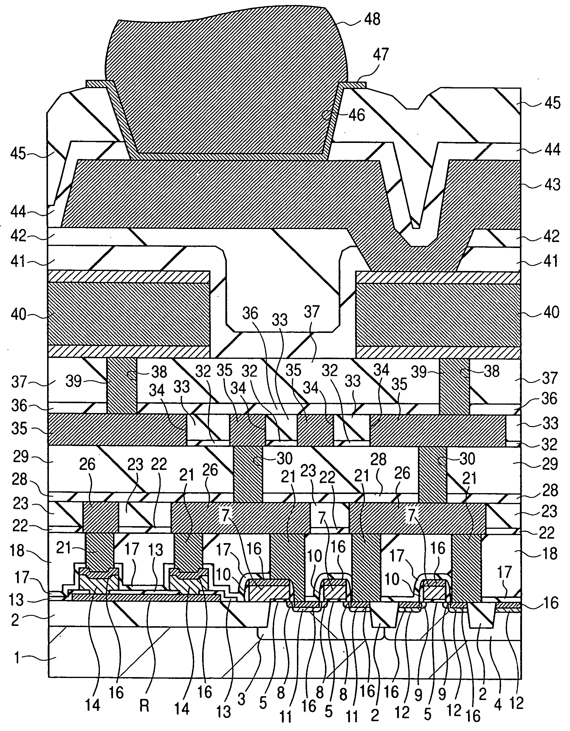
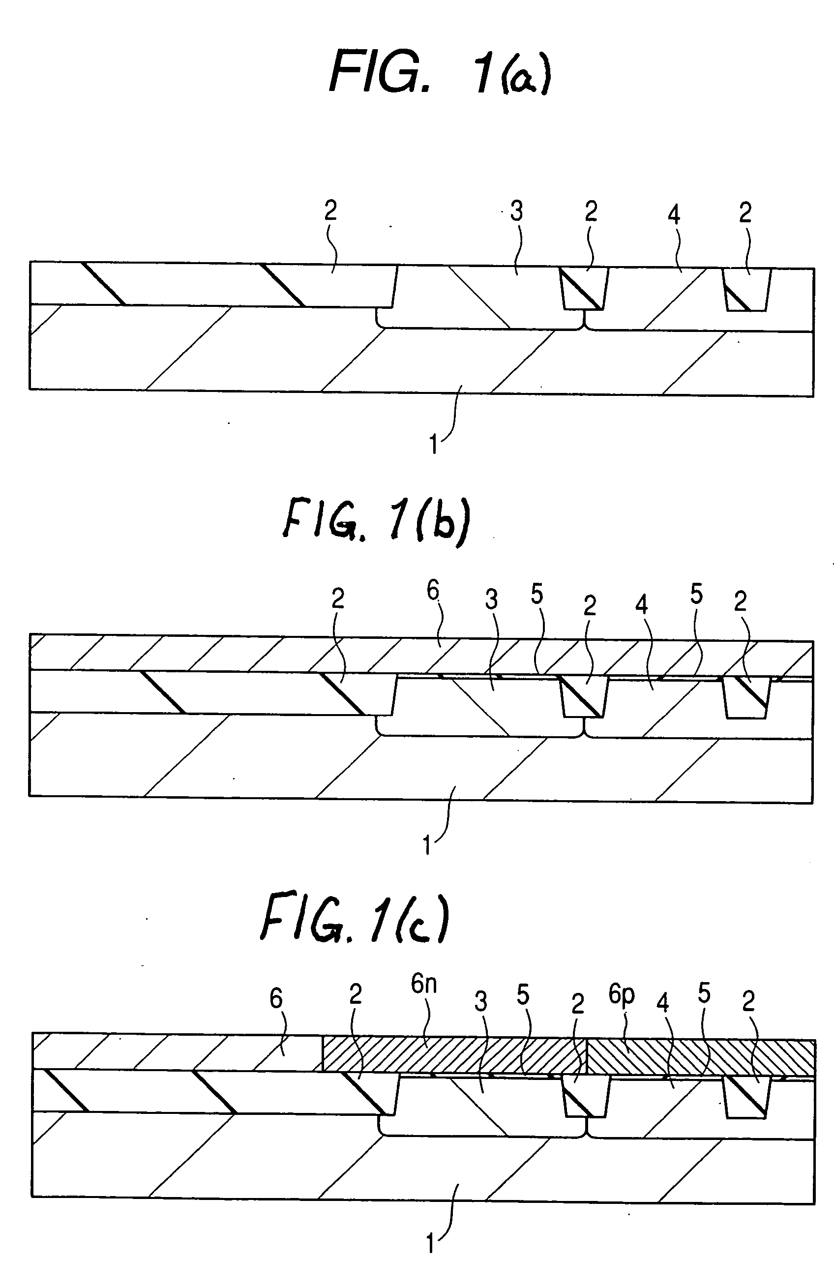
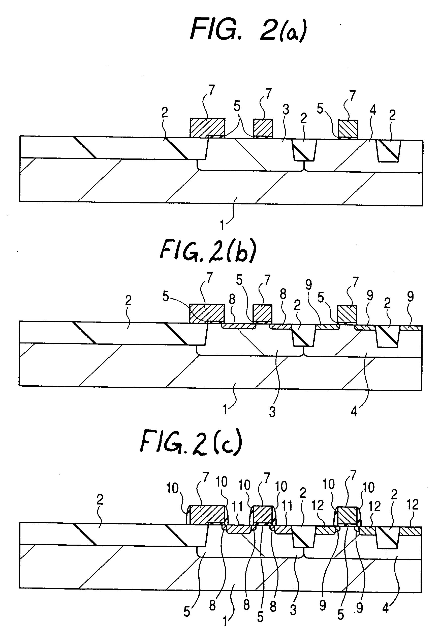
[0169] FIGS. 1(a) to 14 are cross-sectional views illustrating, in the order of steps, a process in the manufacture of a semiconductor device according to Embodiment 1 of the present invention.

[0170] As illustrated in FIG. 1(a), over the main surface of a semiconductor substrate 1, for example, made of p− type single crystal silicon, an element isolation region 2 is formed. This element isolation region 2 can be formed, for example, in the following manner. First, a silicon oxide (SiO) film and a silicon nitride (SiN) film are successively formed over the main surface of the semiconductor substrate 1. Using a patterned photoresist film, the silicon nitride film is etched. With this etched silicon nitride film being used as a mask, a shallow trench is formed in the semiconductor substrate 1. An insulating film, for example, a silicon oxide film is deposited to embed the shallow trench, followed by removal of the silicon oxide film from a region other than the shallow trench by CMP (...

embodiment 2

[0238] The process of manufacture of a DRAM (Dynamic Random Access Memory) according to Embodiment 2 of the invention will next be described in the order of steps based on FIGS. 20 to 42. In each of the drawings illustrating the cross-section of a substrate, a region (memory cell array) wherein a memory cell of a DRAM is to be formed is illustrated on the left side, while a peripheral circuit region is illustrated on the right side.

[0239] As illustrated in FIG. 20, an element isolating trench 102 of about 350 nm depth is defined by photolithography and etching in a semiconductor substrate 101 (hereinafter simply called a“substrate”) which is formed of a p-type single crystal silicon having a specific resistance of about 10 Ωcm. A thin (about 10 nm thick) silicon oxide film 106 is then formed on the inner wall of the element isolating trench 102, for example, by wet oxidation at about 850° C. to 900° C. or dry thermal oxidation at about 1000° C. A silicon oxide film (which will here...


PUM


Abstract

In the manufacture of a semiconductor device having a high-performance and high-reliability, a silicon nitride film 17 for self alignment, which film is formed to cover the gate electrode of a MISFET, is formed at a substrate temperature of 400° C. or greater by plasma CVD using a raw material gas including monosilane and nitrogen. A silicon nitride film 44 constituting a passivation film is formed at a substrate temperature of about 350° C. by plasma CVD using a raw material gas including monosilane, ammonia and nitrogen. The hydrogen content contained in the silicon nitride film 17 is smaller than that contained in the silicon nitride film 44, making it possible to suppress hydrogen release from the silicon nitride film 17.

Description

BACKGROUND OF THE INVENTION [0001] The present invention relates to a semiconductor device and a process of manufacture thereof; and, more particularly, the invention relates to a technique that is effective in producing a highly integrated circuit device that has a high performance and a high reliability. [0002] With a tendency to enhance the performance and increase the degree of miniaturization of a semiconductor device, a self alignment technique that is capable of absorbing mask alignment errors has been employed frequently. [0003] For example, Japanese Patent Application Laid-Open No. Hei 11(1999)-26714 discloses a technique which calls for covering, with a silicon nitride film, gate electrodes of a MISFET (Metal Insulator Semiconductor Field Effect Transistor) constituting the memory cell of a DRAM, forming an interlayer insulating film made of a silicon oxide film, and then forming a plug for connecting source and drain regions of the MISFET. In the processing step of provid...

Claims


Application Information

Patent Timeline
IPC IPC(8): H01L21/00H01L21/02H01L21/318H01L21/60H01L21/768H01L21/8238H01L21/8239H01L21/8242H01L27/06H01L27/108
CPCH01L21/3185H01L21/76816H01L2924/1306H01L21/76828H01L21/76829H01L21/76834H01L21/7685H01L21/76867H01L21/76889H01L21/76895H01L21/76897H01L21/823828H01L21/823871H01L27/0629H01L27/10814H01L27/10888H01L27/10894H01L28/24H01L27/1052H01L24/11H01L2924/00H01L2924/14H01L2224/05569H01L2224/05024H01L2224/05008H01L2224/05009H01L2224/05572H01L2224/05124H01L2224/05166H01L2224/05644H01L24/05H01L21/0217H01L21/02274H10B99/00H10B12/315H10B12/485H10B12/09H01L2924/00014H10B12/00
Inventor FUJIWARA, TSUYOSHIUSHIYAMA, MASAHIROICHINOSE, KATSUHIKOOHASHI, NAOHUMISAITO, TETSUO
Owner RENESAS ELECTRONICS CORP
Why Eureka
Try Eureka