Pressing and breakover process and laminating board structure of circuit board

A circuit board and conduction technology, which is applied in the manufacturing process and structure of circuit boards, can solve product quality problems, high cost of laser drilling blind hole conduction process, hole deformation and other problems, and achieve the effect of low cost

Active Publication Date: 2013-01-02
NETRON SOFT-TECH ZHUHAI CO LTD
View PDF0 Cites 0 Cited by
  • Summary
  • Abstract
  • Description
  • Claims
  • Application Information

AI Technical Summary

Problems solved by technology

In laser drilling, the beam positioning system is extremely important for the accuracy of aperture forming. Although the precise positioning of the beam positioning system is used, due to the influence of other factors, the lack of flame in the hole deformation often occurs, and product quality is easy to occur during the production process. question
On the other hand, the cost of the laser drilling blind hole conduction process is relatively high

Method used


Image

  • Pressing and breakover process and laminating board structure of circuit board
  • Pressing and breakover process and laminating board structure of circuit board
  • Pressing and breakover process and laminating board structure of circuit board

Examples


Embodiment Construction

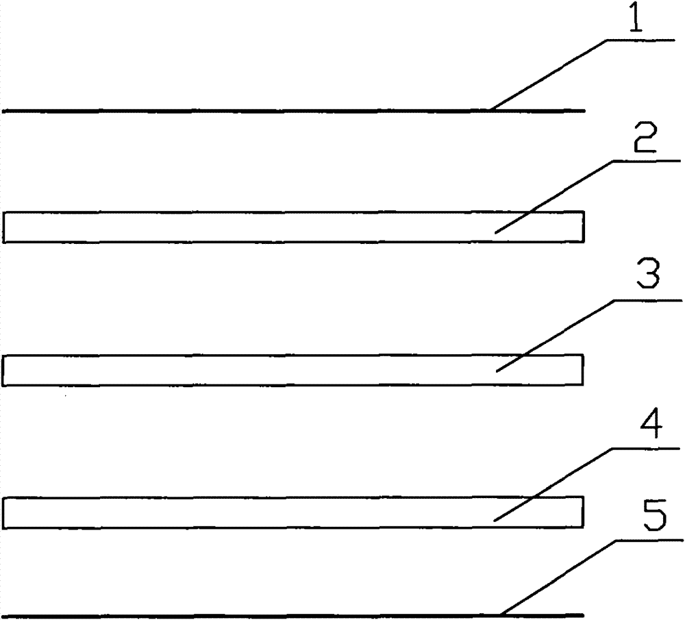
[0029] Such as figure 1 To and image 3 As shown, a press-fit and conduction process of a circuit board includes an inner layer board and an outer layer board prepared by blanking, and the processing technology mainly includes the following steps,

[0030] A. Fabrication of the inner layer board circuit. After the inner layer board is coated with copper, the designed circuit diagram is transferred to the board through the film, and then the required circuit is obtained by etching the inner layer board;

[0031] B, outer layer plate pressing, described outer layer plate and the inner layer plate obtained through step A are pressed;

[0032] C, drilling, the multi-layer board obtained in step B is drilled, so that the corresponding lines on the upper and lower positions of the circuit board are conducted by drilling;

[0033] D, electroplating, make the hole wall of step C conduction by electroplating;

[0034] E. Printing, through printing, the holes on the circuit board are...


PUM


Abstract

The invention relates to a pressing and breakover process of a circuit board, comprising an inner-layer board and an outer-layer board which are made through blanking. The machining process mainly comprises the following steps of: making an inner-layer board circuit, pressing the outer-layer board, drilling, electroplating, printing, laminating boards, pressing laminating boards, making an outer-layer board circuit and printing with preventing weld paint; and then performing word printing, surface processing and shape machining for the obtained circuit board to obtain a finished product. The laminating board structure of the circuit board comprises a basal board which is formed by machining the inner-layer board and the outer-layer board through the steps, the upper surface and the under surface of the basal board are respectively provided with a layer of steel board, and the upper surface and the under surface of the steel board are respectively provided with a layer of kraft paper. Compared with the prior art, the invention has the characteristics that printing is connected with breakover, and the printing laminating boards are coherent together; relative to a laser blinding hole drilling process, the cost of the process is lower; and the laser blinding hole drilling process is changed into a pressing process subjected to printing, and normal breakover can be achieved after connection.

Description

technical field [0001] The invention relates to a manufacturing process and structure of a circuit board, in particular to a pressing and conduction process of the circuit board and a laminated structure of the circuit board. Background technique [0002] With the rapid development of microelectronics technology, the wide application of large-scale and ultra-large-scale integrated circuits, and the progress of micro-assembly technology, the manufacture of printed circuit boards is developing towards lamination and multi-function. PCB (Printed Circuit Board) needs to drill holes before bonding multilayer boards. Drilling holes can align the corresponding copper wires on the upper and lower positions of the circuit board, and then perform hole electroplating to make the hole walls with copper and make the holes conduct. The methods used in the existing PCB microhole processing generally include mechanical drilling and laser drilling. [0003] At present, the production proces...

Claims


Application Information

Patent Timeline
Patent Type & Authority Patents(China)
IPC IPC(8): H05K3/00H05K3/46
Inventor 刘惠民彭勇强陈明祺
Owner NETRON SOFT-TECH ZHUHAI CO LTD
Why Eureka
Try Eureka