Wafer defect detecting method
A detection method and wafer technology, applied in semiconductor/solid-state device testing/measurement, etc., can solve problems such as re-examination, achieve the effect of ensuring service life and improving scanning efficiency
- Summary
- Abstract
- Description
- Claims
- Application Information
AI Technical Summary
Problems solved by technology
Method used
Image


Examples
Embodiment Construction
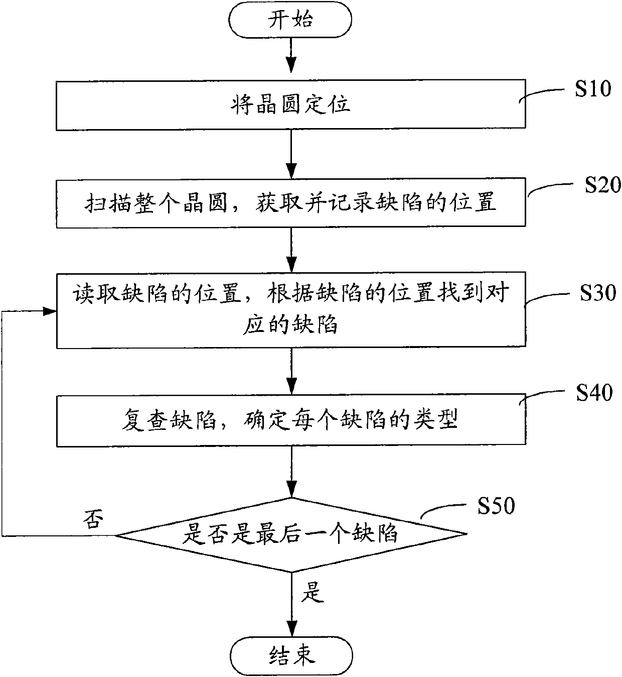
[0018] Such as figure 1 As shown, it is a processing flowchart of a wafer defect detection method. The method comprises the steps of:
[0019] S10: Positioning the wafer: acquiring the apex of the notch of the wafer, and adjusting the position of the wafer to move the notch to a predetermined position and direction.
[0020] Such as figure 2 As shown, is a schematic diagram of the exterior of the wafer 10 . The wafer 10 is circular and has a notch 11 on its edge, and the notch 11 can be used for positioning the wafer 10 in processes such as photolithography. When using the notch 11 to position the wafer 10 , a detection step of the notch 11 is involved, and the apex 12 of the notch 11 is determined. In order to facilitate the use of defect positions obtained by scanning, the wafer 10 is placed in the same orientation each time it enters the machine, so that the position information obtained by scanning can be used directly in re-inspection without conversion.
[0021] S2...
PUM
 Abstract
Description
Claims
Application Information