

Load lock chamber
A sampling chamber, vacuum technology, applied in the direction of electrical components, semiconductor/solid-state device manufacturing, circuits, etc., can solve problems such as bending and cracking of the main body of the vacuum sampling chamber
- Summary
- Abstract
- Description
- Claims
- Application Information
AI Technical Summary
Problems solved by technology
Method used
Image

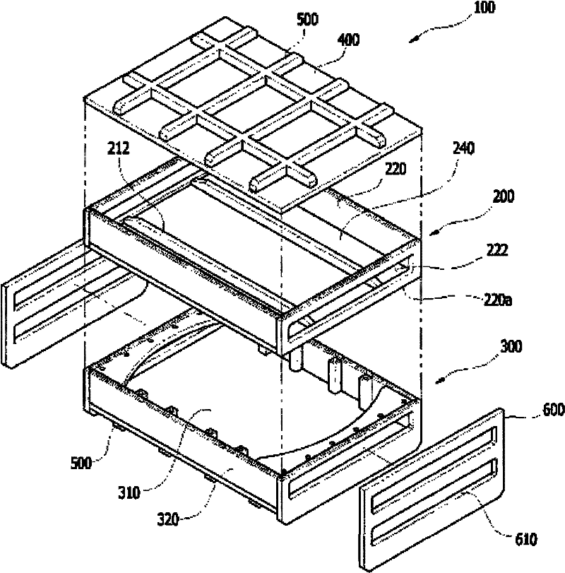
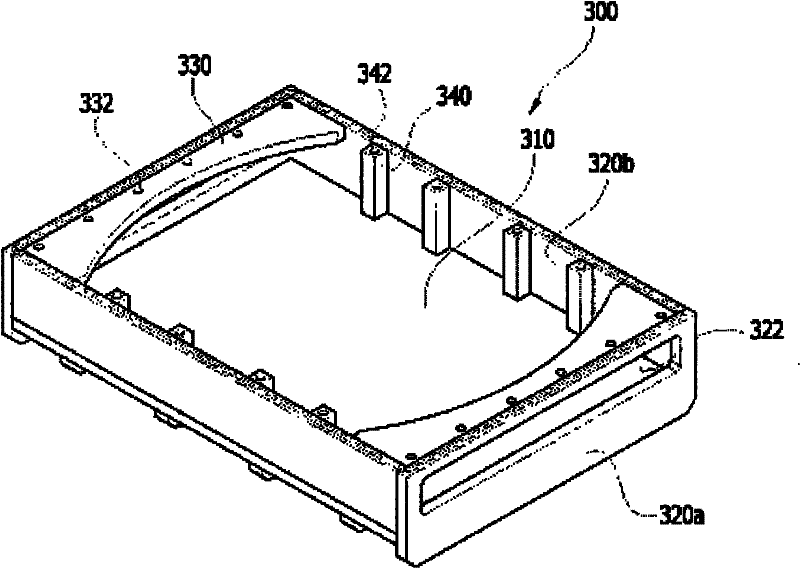
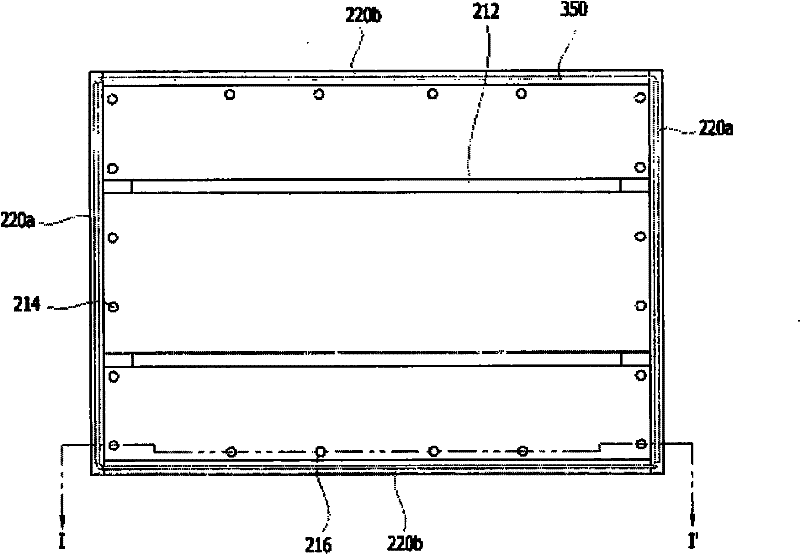
Examples
Embodiment Construction
[0028] Hereinafter, preferred embodiments of the present invention will be described in detail with reference to the accompanying drawings. The above features and effects of the present invention will become clearer through the following detailed description in conjunction with the accompanying drawings, and those skilled in the art of the present invention can easily implement the technical idea of the present invention. The present invention is not limited to the following embodiments, but can be realized in other ways. The role of each embodiment described in this specification is to disclose the technical content more completely and fully convey the technical ideas and features of the present invention to those skilled in the art. In the drawings, in order to clearly illustrate the present invention, the thickness of each device or film (layer) and region is exaggerated, and each device may include various additional devices not described in this specification.
[0029]...
PUM
 Abstract
Description
Claims
Application Information