Wafer processing method

A processing method and wafer technology, which is applied in the direction of electrical components, semiconductor/solid-state device manufacturing, circuits, etc., can solve the problems that the laser beam cannot form a modified layer, and cannot be divided into wafers.

Inactive Publication Date: 2016-03-09
DISCO CORP
View PDF8 Cites 0 Cited by
  • Summary
  • Abstract
  • Description
  • Claims
  • Application Information

AI Technical Summary

Problems solved by technology

[0008] However, since the Nd:YAG pulsed laser has a wavelength of 1064nm close to the optical absorption end of silicon, part of the laser beam is absorbed in the region sandwiching the focal point, and a sufficient modified layer cannot be formed, and the wafer cannot be divided into individual parts. The case of the device chip

Method used


Image

  • Wafer processing method
  • Wafer processing method
  • Wafer processing method

Examples


Embodiment Construction

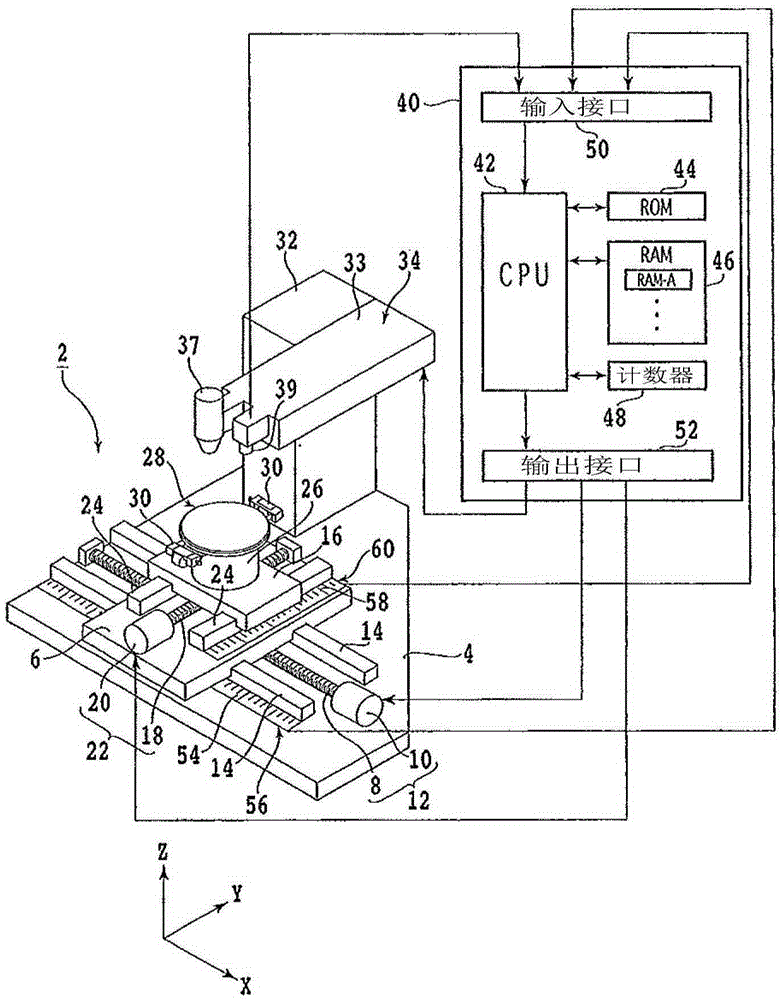
[0031] Hereinafter, embodiments of the present invention will be described in detail with reference to the drawings. when referring to figure 1 , a schematic perspective view of a laser processing apparatus 2 suitable for implementing the wafer processing method of the present invention is shown.

[0032] The laser processing device 2 includes a first slider 6 mounted on a stationary base 4 so as to be movable in the X-axis direction. The first slider 6 moves along a pair of guide rails 14 in the machining feed direction, that is, the X-axis direction, via a machining feed mechanism 12 composed of a ball screw 8 and a pulse motor 10 .

[0033] The second slider 16 is mounted on the first slider 6 so as to be movable in the Y-axis direction. That is, the second slider 16 moves along the pair of guide rails 24 in the index feed direction, that is, the Y-axis direction, via the index feed mechanism 22 constituted by the ball screw 18 and the pulse motor 20 .

[0034] On the se...


PUM


Abstract

The invention provides a wafer processing method for processing the silicon-formed wafer formed through a plurality of division-presetting lines dividing a plurality of devices on a front surface. The invention comprises the following steps: a wave length setting step for setting the wave length of a permeable pulse laser beam in a range of 1300nm-1400nm; a modification layer forming step, wherein a luminous spot of the pulse laser beam is positioned in the wafer, the modification layer is formed in the wafer through emission of the pulse laser beam from the back of the wafer to an area corresponding to the division-presetting lines; a dividing step for applying external force on wafer to use the modification layer as a start to divide the wafer along the division-presetting lines; wherein in the modification layer forming step, the brittle part of the device formed by the device being adjacent to the division-presetting lines to position the luminous spot of the pulse laser beam, and the brittle part is damaged by the emitting of pulse laser beam becaused of scattering.

Description

technical field [0001] The present invention relates to a method of processing a wafer. After a modified layer is formed inside the wafer by irradiating a pulsed laser beam of a wavelength that is transparent to the wafer, an external force is applied to the wafer to divide the wafer into a plurality of wafers starting from the modified layer. device chip. Background technique [0002] Multiple devices such as IC and LSI are formed on the front side of a silicon wafer (hereinafter, sometimes simply referred to as a wafer) by dividing predetermined lines, and the silicon wafer is divided into individual device chips by a processing device, and the divided device chips are widely used. Used in various electronic devices such as mobile phones and personal computers. [0003] For dividing wafers, a dicing method using a cutting device called a dicing saw is widely used. In the dicing method, a cutting tool made of metal or resin with abrasive grains such as diamond solidified ...

Claims


Application Information

Patent Timeline
Patent Type & Authority Applications(China)
IPC IPC(8): H01L21/268H01L21/78
CPCH01L21/268H01L21/78
Inventor 古田健次
Owner DISCO CORP
Why Eureka
Try Eureka