Chip-on-board package structure and method for manufacturing the same

A technology of packaging structure and carrier board, which is applied in the direction of electrical components, circuits, semiconductor devices, etc., can solve the problems of plastic overflow, poor light extraction rate, complicated manufacturing process, etc., to avoid colloid overflowing the packaging area, reduce the internal resistance of the chip carrier board, The effect of avoiding colloid waste

Inactive Publication Date: 2011-06-29
YIWANG GROUP
View PDF0 Cites 1 Cited by
  • Summary
  • Abstract
  • Description
  • Claims
  • Application Information

AI Technical Summary

Problems solved by technology

However, the manufacturing process of the above method is very complicated and its light extraction rate is poor. Especially in the manufacturing process, when plastic is used for sealing at the end, since it is encapsulated by a large-area one-time coating method, the plastic will overflow the packaging area.
In addition, the internal resistance will increase due to the increase in the number of substrate layers due to the

Method used


Image

  • Chip-on-board package structure and method for manufacturing the same
  • Chip-on-board package structure and method for manufacturing the same
  • Chip-on-board package structure and method for manufacturing the same

Examples


Embodiment Construction

[0013] In order to fully understand the purpose, features and effects of the present invention, the present invention will be described in detail through the following specific embodiments and accompanying drawings, as follows:

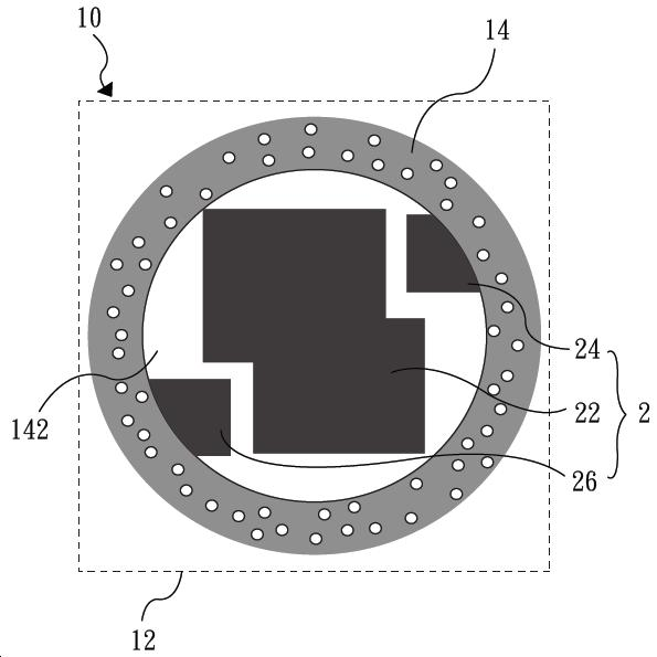
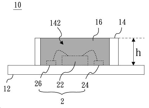
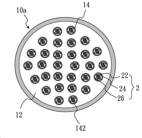
[0014] Please also refer to figure 1 and figure 2 . in, figure 1 It is a structural schematic diagram of a chip carrier packaging structure according to an embodiment of the present invention; figure 2 is used to illustrate the figure 1 The cross-sectional schematic diagram of the chip carrier package structure. In the figure, the chip carrier package structure 10 is used to package a light emitting diode 2 . Wherein, the LED 2 includes a bare chip 22 and two electrodes 24 , 26 . The chip carrier packaging structure 10 includes a substrate 12 , a sealing wall 14 and a sealing layer 16 . Wherein, the substrate 12 may further include at least one conductive layer (not shown in the figure) and an insulating layer (not shown in the figure), and t...


PUM


Abstract

The invention discloses a chip-on-board (ChipOnBoard, COB) package structure, which comprises a substrate, a light emitting diode, a seal wall and a seal layer. The light emitting diode is arranged on one side of the substrate. The seal wall is arranged at the periphery of the light emitting diode and a package area is formed by the seal wall and the periphery of the light emitting diode. The seal wall has a package height on the substrate to form a package area equipped with the above package height. The seal layer is arranged in the package area to seal the light emitting diode inside the package area. By utilizing the invention, glue is prevented from overflowing out of the package area during the seal process. Meanwhile, the internal resistance and the manufacture cost are low. In addition, a process method corresponding to the package structure of the chip-on-board is also provided.

Description

technical field [0001] The invention relates to a chip carrier board (COB) packaging structure and its manufacturing method, especially the packaging structure and method for packaging single or multiple light emitting diodes. Background technique [0002] The conventional LED chip carrier board (COB) packaging technology utilizes injection molding, external mounting, splint type or concave cup type of operation to carry out the circuit layout (layout) of multiple light emitting diodes, and then multiple light emitting diodes For one-time packaging. However, the manufacturing process of the above method is very complicated and its light extraction rate is poor, especially in the manufacturing process, when plastic is used for sealing at the end, since it is encapsulated by a large-area one-time coating method, the plastic will overflow the packaging area. In addition, the internal resistance will increase due to the increase in the number of layers of the substrate due to t...

Claims


Application Information

Patent Timeline
IPC IPC(8): H01L33/48H01L33/54H01L33/00
Inventor 刘进财何沛錞
Owner YIWANG GROUP
Why Eureka
Try Eureka