Liquid crystal device, method of controlling liquid crystal device, and electronic apparatus

A liquid crystal device and control circuit technology, applied in the direction of cathode ray tube indicators, instruments, static indicators, etc., can solve the problem of continuing and achieve the effect of suppressing flickering

Inactive Publication Date: 2011-08-03
SEIKO EPSON CORP
View PDF5 Cites 2 Cited by
  • Summary
  • Abstract
  • Description
  • Claims
  • Application Information

AI Technical Summary

Problems solved by technology

[0004] However, even if the voltage applied to the electrodes is adjusted so that the flicker is minimized, a DC component may be applied to the liquid crystal element due to changes in time, etc.
According to the invention described in Patent Document 1, since the user can adjust the voltage, the voltage of the electrode can be readjusted after shipment, but the user is required to perform operations different from normal operations such as adjustment operations.
In addition, since the electrode voltage will not be readjusted unless the user readjusts, the flickering state may continue.

Method used


Image

  • Liquid crystal device, method of controlling liquid crystal device, and electronic apparatus
  • Liquid crystal device, method of controlling liquid crystal device, and electronic apparatus
  • Liquid crystal device, method of controlling liquid crystal device, and electronic apparatus

Examples


no. 1 Embodiment approach

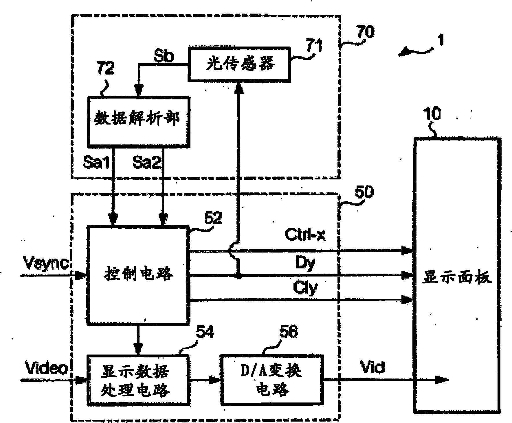
[0041] figure 1 It is a block diagram showing the configuration of the electro-optical device 1 according to the first embodiment of the present invention.

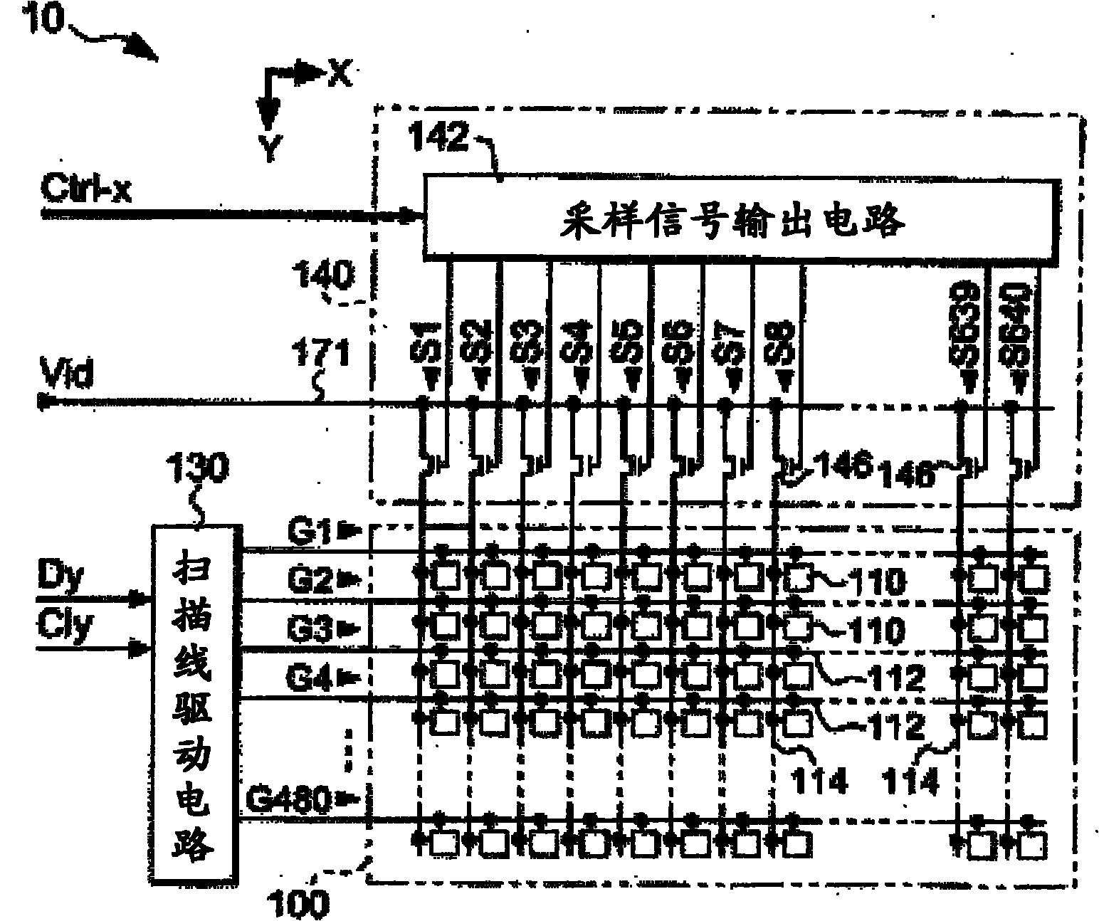
[0042] Such as figure 1 As shown, the electro-optical device 1 is roughly divided into a display panel 10 , a processing circuit 50 , and a detection circuit 70 . Among them, the processing circuit 50 as a circuit module for controlling the operation of the display panel 10 includes: a control circuit 52, a display data processing circuit 54, and a D / A conversion circuit 56, and is connected to the display panel 10 through, for example, an FPC (flexible printed circuit) substrate. connect. In addition, the detection circuit 70 includes an optical sensor 71 and a data analysis unit 72 . In addition, the electro-optical device 1 is an example of a liquid crystal device that displays images using liquid crystals.

[0043] The control circuit 52 generates various control signals for controlling the display panel 10 in syn...

no. 2 Embodiment approach

[0121] Next, an electro-optical device 1 according to a second embodiment of the present invention will be described. The electro-optical device 1 according to the second embodiment is the same as that of the first embodiment in terms of hardware configuration. The electro-optical device 1 according to the second embodiment is different from the electro-optical device 1 according to the first embodiment in that the process performed by the control circuit 52 is different. Therefore, the following description will focus on this point of difference.

[0122] Figure 15 It is a flowchart showing the flow of processing performed by the control circuit 52 according to the second embodiment. In addition, in the control circuit 52 , the processing from the start of the drive of the display panel 10 to step SB1 is the same as that of the first embodiment.

[0123] First, the control circuit 52 acquires the signal Sa1 and the signal Sa2 supplied from the data analysis unit 72 (step ...

no. 3 Embodiment approach

[0135]Next, an electro-optical device 1 according to a third embodiment of the present invention will be described. The electro-optical device 1 according to the third embodiment is the same as that of the first embodiment in terms of hardware configuration. The electro-optical device 1 according to the third embodiment is different from the electro-optical devices 1 according to the first and second embodiments in that the processing performed by the control circuit 52 is different. Therefore, the following description will focus on this point of difference.

[0136] Figure 17 It is a flowchart showing the flow of processing performed by the control circuit 52 according to the third embodiment. The third embodiment differs from the second embodiment in that it has step SB2a.

[0137] Figure 18 It is a flowchart showing the flow of the set value setting process performed in step SB2a.

[0138] First, the control circuit 52 acquires the signal Sa1 and the signal Sa2 (ste...


PUM


Abstract

The present invention relates to a liquid crystal device, a method of controlling the liquid crystal device and an electronic apparatus. In a case that a brightness of a pixel when the pixel maintains a voltage of the negative polarity is greater than that when the pixel maintains a voltage of the positive polarity and a brightness difference is more than or equal to a threshold value, a trigger pulse (Dyb) is output in timing delaying a time (T). Otherwise, in a case that the brightness of the pixel when the pixel maintains a voltage of the positive polarity is greater than that when the pixel maintains a voltage of the negative polarity and a brightness difference is more than or equal to the threshold value, the trigger pulse (Dyb) is output in timing being early to the time (T). By means of alternately switching a state of outputting the trigger pulse (Dyb) delaying the time (T) and a state of outputting the trigger pulse (Dyb) being early to the time (T), the difference between brightness of the pixel when the pixel maintains a voltage of the positive polarity and brightness of the pixel when the pixel maintains a voltage of the negative polarity is gradually changed in a predetermined range so as to restrain flashing. Thereby, DC components are prevented from applying to the liquid crystal without regulation operation of a user so as to restrain flashing.

Description

technical field [0001] The present invention relates to techniques for suppressing occurrence of flicker in electro-optical devices. Background technique [0002] A liquid crystal element used in a liquid crystal display device has a structure in which liquid crystal is sandwiched between two electrodes, but the liquid crystal deteriorates when a DC component is applied. Therefore, in liquid crystal display devices, liquid crystal elements are generally driven by alternating current. However, in the case of only AC driving, there is known a technique that minimizes flicker, that is, minimizes flicker, that is, minimizes flicker, that is, minimizes the transmittance (brightness) generated by applying a voltage of positive polarity and that based on negative polarity. In order to minimize the difference in transmittance due to the application of a permanent voltage, the voltage applied to one electrode of the liquid crystal element is adjusted (for example, refer to Patent Do...

Claims


Application Information

Patent Timeline
Patent Type & Authority Applications(China)
IPC IPC(8): G09G3/36
CPCG09G5/10G09G3/3614G09G3/3648G09G3/3688G09G2320/0247G09G2360/16
Inventor 佐佐木仁饭坂英仁水迫和久
Owner SEIKO EPSON CORP
Why Eureka
Try Eureka