Optical semiconductor module and method for assembling the same
A technology of optical semiconductors and assembly methods, which is applied in the direction of semiconductor laser optical devices, semiconductor lasers, light guides, etc., can solve the problems that hinder the miniaturization of optical semiconductor components, achieve stable optical coupling efficiency, and suppress the reduction of output light intensity.
- Summary
- Abstract
- Description
- Claims
- Application Information
AI Technical Summary
Problems solved by technology
Method used
Image
Examples
Embodiment 1
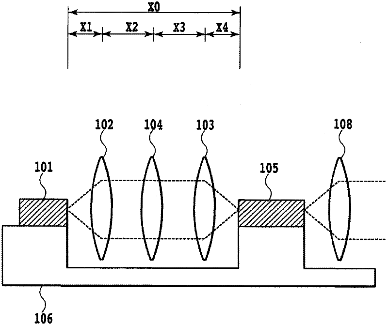
[0040] figure 1 Example 1 of the present invention is shown. Such as figure 1 As shown, the optical semiconductor module of this embodiment has a first lens 102, a second lens 103, and a third lens 104, and a semiconductor laser 101 and a semiconductor optical modulator 105, respectively, which are waveguide-type optical semiconductor elements. The semiconductor laser 101 and The semiconductor light modulator 105 is an optical semiconductor element mounted on a bracket 106, and the positions of the first lens 102, the second lens 103, and the third lens 104 are adjusted so that the light emitted from the semiconductor laser 101 can be coupled with a low loss. at the position of the semiconductor light modulator 105 .
[0041] Here, a Fabry-Perot laser with an oscillation wavelength of 1.55 μm is used as the semiconductor laser 101 , and an electrolytic absorption (EA) modulator capable of supporting the 1.5 μm band is used as the semiconductor optical modulator 105 .
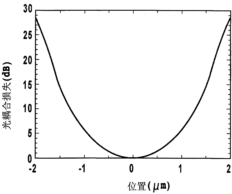
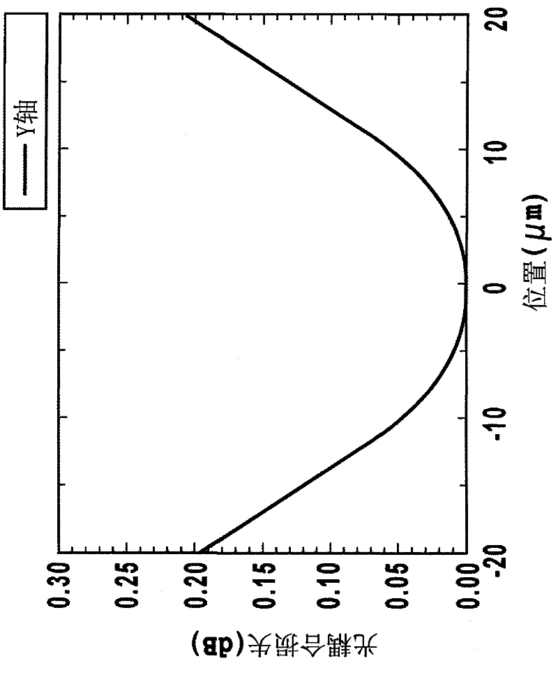
[004...
Embodiment 2
[0057] In Example 2, the difference from Example 1 is that YAG laser welding is used when fixing the lens. Compared with the case of using epoxy resin to fix the lens, when the lens is fixed by YAG laser welding, the positional displacement of the lens is less, usually about 1 μm. Therefore, since the amount of correction by the third lens is small, the optical axes can be easily aligned.
[0058] In addition, in the case of using an adhesive such as epoxy resin, there are problems such as deformation of the adhesive such as epoxy resin over time after fixing, resulting in misalignment of the optical axis, but in the case of YAG laser welding There will be no such problems, so it has excellent reliability.
[0059] Figure 5 Shows the second embodiment of the present invention. Such as Figure 5 As shown, the first lens 502, the second lens 503, and the third lens 504 of the optical semiconductor assembly of this embodiment, and the semiconductor laser 501 and the semicond...
Embodiment 3
[0073] Figure 7 An optical semiconductor module having the same optical system as that of Example 2 as Example 3 is shown. The optical semiconductor assembly of this embodiment has a first lens 702, a second lens 703, and a third lens 704, and a semiconductor laser 701 and a semiconductor optical modulator 705, which are respectively waveguide-type optical semiconductor elements. The laser 705 is an optical semiconductor element mounted on a bracket 706, and the positions of the first lens 702, the second lens 703, and the third lens 704 are adjusted so that the light emitted from the semiconductor laser 701 is coupled to the semiconductor light modulator with low loss. device 705. The first lens 702, the second lens 703, and the third lens 704 are housed in metal cases 712, 713, and 714, respectively.
[0074] Here, a DFB laser with an oscillation wavelength of 1.55 μm is used as the semiconductor laser 701 , and a Mach-Zehnder (MZ) modulator capable of supporting the 1.55...
PUM
 Abstract
Description
Claims
Application Information
 - R&D
- Intellectual Property
- Life Sciences
- Materials
- Tech Scout
- Unparalleled Data Quality
- Higher Quality Content
- 60% Fewer Hallucinations
Browse by: Latest US Patents, China's latest patents, Technical Efficacy Thesaurus, Application Domain, Technology Topic, Popular Technical Reports.
© 2025 PatSnap. All rights reserved.Legal|Privacy policy|Modern Slavery Act Transparency Statement|Sitemap|About US| Contact US: help@patsnap.com


