Method for improving safety insulation voltage endurance of light-emitting diode (LED) integrating face light source
A technology of insulation withstand voltage and surface light source, which is applied in the direction of electrical components, circuits, semiconductor devices, etc., and can solve the problems that cannot reliably meet the requirements of insulation withstand voltage
- Summary
- Abstract
- Description
- Claims
- Application Information
AI Technical Summary
Problems solved by technology
Method used
Image
Examples
Embodiment 1
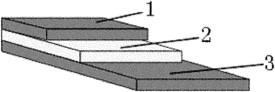
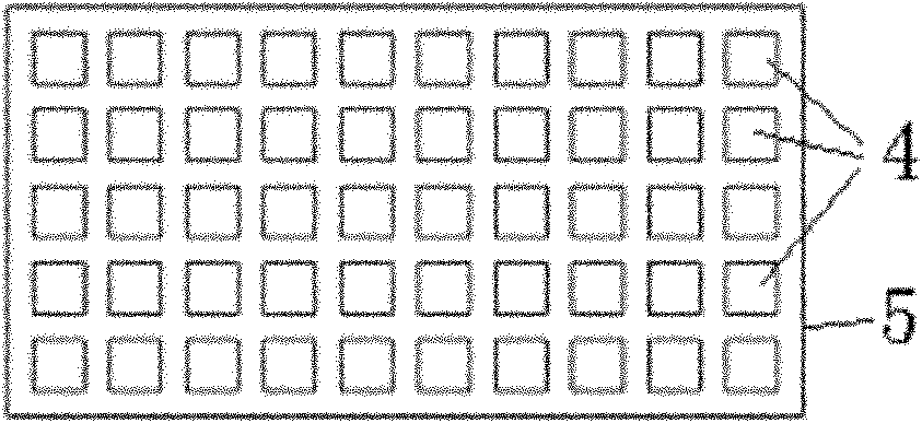
[0030] refer to figure 2 , is a double-sided aluminum oxide ceramic copper-clad laminate 5 bracket for carrying 50 LEDs. According to the power of a single LED chip, it can form a 25W-50W integrated surface light source, with a total size of 31mm×16mm. The bottom layer is all copper, the middle insulation layer 2 is made of aluminum oxide ceramic layer with a thickness of 0.38mm, and the upper layer is made of 50 LED copper foil islands 4. A 0.075-0.1um silver layer can be plated to facilitate the bonding of a single LED chip with conductive silver paste. The width of the partition wall where the copper layer is corroded is 1mm, and the edge of the whole board is left with a 1mm isolation strip for corroding the copper layer.
Embodiment 2
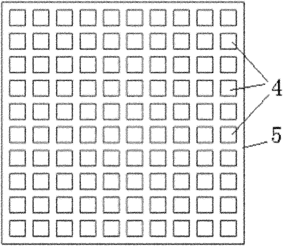
[0032] refer to image 3 , to carry 100 LED double-sided aluminum nitride ceramic copper-clad laminate 5 brackets, considering high-power heat dissipation, aluminum nitride ceramic copper-clad laminate 5 is used for the bracket, according to the power of a single LED chip, it can form a 100W-200W integrated surface light source , The total size is 31mm×31mm. The bottom layer is all copper, and the middle insulating layer 2 is made of 0.25mm thick aluminum nitride ceramic insulating layer. The thermal conductivity of aluminum nitride is as high as 170-220W / mK, which can further reduce thermal resistance and meet high-power heat dissipation requirements. Make 100 LED bonding copper foil islands 4 on the upper layer. The single island size is 2mm×2mm, and the copper foil island 4 with a thickness of 0.3mm can be plated with 0.075-0.1um silver layer to facilitate the bonding of a single LED chip with conductive silver paste. Then, the width of the partition wall where the copper ...
PUM
| Property | Measurement | Unit |
|---|---|---|
| thickness | aaaaa | aaaaa |
| dielectric strength | aaaaa | aaaaa |
| thickness | aaaaa | aaaaa |
Abstract
Description
Claims
Application Information


