Device and method for managing semiconductor cleaning solution

A technology for managing devices and cleaning liquids, which is applied in the fields of cleaning methods, cleaning methods and utensils using liquids, semiconductor/solid-state device manufacturing, etc., which can solve the problem that cleaning liquids cannot be automatically managed, cannot meet production needs, and semiconductor cleaning devices cannot be cleaned. Process flow and other issues

Active Publication Date: 2011-10-05
BEIJING SEVENSTAR ELECTRONICS CO LTD
View PDF2 Cites 28 Cited by
  • Summary
  • Abstract
  • Description
  • Claims
  • Application Information

AI Technical Summary

Problems solved by technology

[0002] At present, in the semiconductor cleaning industry, the semiconductor cleaning device includes a reaction chamber control device and a transmission control device. The reaction chamber control device is used to realize the cleaning process of the reaction chamber, and the transmission control device is used to transfer silicon wafers to the reaction chamber. The cleaning liquid used in the cleaning process cannot be managed automatically. When operating the semiconductor cleaning device, a technician must manage the cleaning liquid, which leads to the failure of the semiconductor cleaning device without technical personnel to manage the cleaning liquid. Unable to carry out continuous cleaning process and unable to meet current production needs

Method used


Image

  • Device and method for managing semiconductor cleaning solution
  • Device and method for managing semiconductor cleaning solution
  • Device and method for managing semiconductor cleaning solution

Examples


Embodiment Construction

[0028] The specific implementation manners of the present invention will be further described in detail below in conjunction with the accompanying drawings and embodiments. The following examples are used to illustrate the present invention, but are not intended to limit the scope of the present invention.

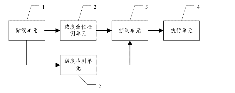
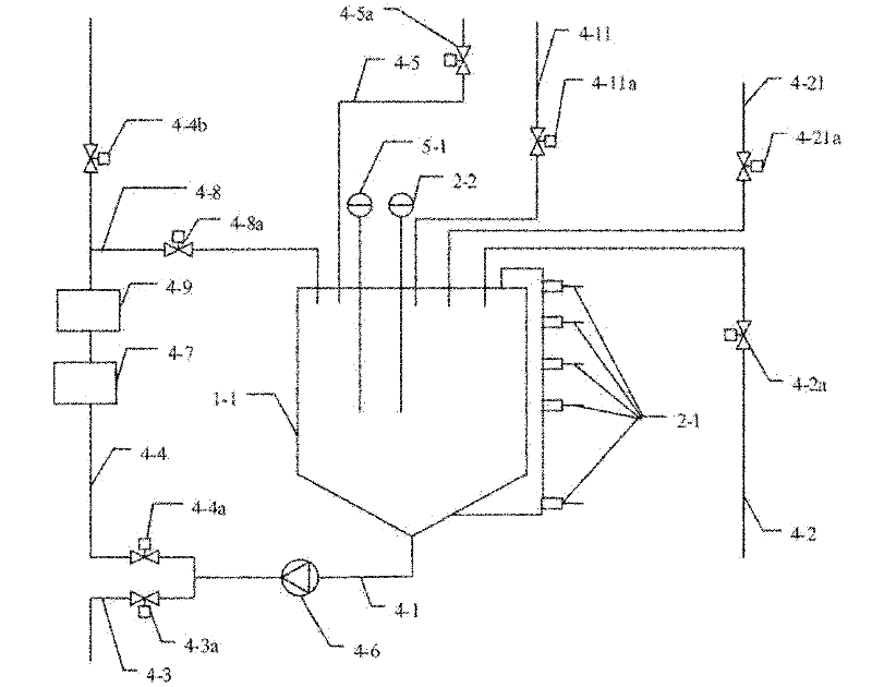
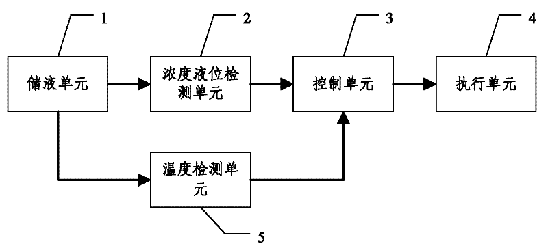
[0029] figure 1 It is a structural block diagram of a semiconductor cleaning liquid management device according to an embodiment of the present invention, including: a liquid storage unit 1, a concentration liquid level detection unit 2, a control unit 3 and an execution unit 4 connected in sequence,

[0030] The liquid storage unit 1 is used to store cleaning liquid;

[0031] The concentration and liquid level detection unit 2 is used to detect the concentration and liquid level of the cleaning liquid in the liquid storage unit 1, and transmit the detected concentration data and liquid level data to the control unit 3;

[0032] The control unit 3 is configured to genera...


PUM


Abstract

The invention discloses a device for managing a semiconductor cleaning solution. The device comprises a solution storage unit, a concentration and liquid level detection unit, a control unit and a performing unit, wherein the solution storage unit is used for storing the cleaning solution; the concentration and liquid level detection unit is used for detecting the concentration and the liquid level of the cleaning solution in the solution storage unit, and transmitting detected concentration data and detected liquid level data to the control unit; the control unit is used for generating corresponding control signals according to the concentration data and the liquid level data, and transmitting the control signals to the performing unit; and the performing unit is used for discharging the cleaning solution of the solution storage unit, compensating chemical agent and water of the solution storage unit, replacing the cleaning solution of the solution storage unit, recycling the cleaning solution of a reaction cavity body and supplying the cleaning solution to the reaction cavity body according to the control signals. The device for managing the semiconductor cleaning solution is combined with a reaction cavity body control device, so automatic management of the cleaning solution and continuous cleaning process in the absence of a technician for managing the cleaning solution are realized.

Description

technical field [0001] The invention relates to the technical field of semiconductor cleaning, in particular to a semiconductor cleaning liquid management device and method. Background technique [0002] At present, in the semiconductor cleaning industry, the semiconductor cleaning device includes a reaction chamber control device and a transmission control device. The reaction chamber control device is used to realize the cleaning process of the reaction chamber, and the transmission control device is used to transfer silicon wafers to the reaction chamber. The cleaning liquid used in the cleaning process cannot be managed automatically. When operating the semiconductor cleaning device, a technician must manage the cleaning liquid, which leads to the failure of the semiconductor cleaning device without technical personnel to manage the cleaning liquid. The continuous cleaning process cannot be carried out, and the current production needs cannot be met. Contents of the in...

Claims


Application Information

Patent Timeline
Patent Type & Authority Applications(China)
IPC IPC(8): H01L21/00B08B3/00
Inventor 郭训容吴仪裴立坤昝威
Owner BEIJING SEVENSTAR ELECTRONICS CO LTD
Why Eureka
Try Eureka