Liquid crystal display and method for manufacturing liquid crystal display

A technology of liquid crystal display and liquid crystal layer, applied in instruments, light guides, optics, etc., can solve the problems of difficult to achieve high transmittance, liquid crystal molecular orientation, etc., achieve good voltage response characteristics, prevent transmittance reduction, and high transmittance.

Active Publication Date: 2011-10-12
SONY CORP
View PDF12 Cites 34 Cited by
  • Summary
  • Abstract
  • Description
  • Claims
  • Application Information

AI Technical Summary

Problems solved by technology

[0008] However, in the above method, although the voltage response characteristic can be improved, the voltage is not applied to the portion of the liquid crystal layer corresponding to the slit (the portion is directly above the slit), and it is difficult to align the liquid crystal molecules (impossible to tilt )
Therefore, a black line (a part where the amount of light transmission is small) is generated corresponding to the position of the slit, and there is a problem that it is difficult to achieve a high transmittance.

Method used


Image

  • Liquid crystal display and method for manufacturing liquid crystal display
  • Liquid crystal display and method for manufacturing liquid crystal display
  • Liquid crystal display and method for manufacturing liquid crystal display

Examples


no. 1 example

[0065] - First Example (Measurement Results of Transmittance in Case of Different Step Heights of Concave and Convex Structures)

[0066] -Second Example (Measurement Results of Transmittance in Case of Different Widths of Upper Surfaces in Modification 3)

[0067] - Third Example (Measurement Results of Transmittance in the Case of Different Step Heights in Modification 3)

Embodiment approach

[0069] Structure of LCD 1

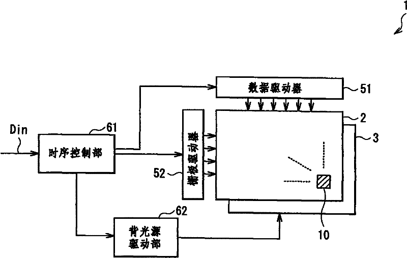
[0070] figure 1 The overall structure of a liquid crystal display (liquid crystal display 1) according to one embodiment of the present invention is shown. The liquid crystal display 1 includes, for example, a liquid crystal display panel 2 , a backlight 3 , a data driver 51 , a gate driver 52 , a timing control unit 61 and a backlight driver 62 , and displays an image based on an external input signal Din.

[0071] The backlight 3 is a light source that irradiates light to the liquid crystal display panel 2 , and is arranged on the back side of the liquid crystal display panel 2 (on the surface on the polarizing plate 19 side to be mentioned later). The backlight 3 includes, for example, LEDs (Light Emitting Diodes), CCFLs (Cold Cathode Fluorescent Lamps), and the like. The backlight driving section 62 controls the lighting operation (light emitting operation) of the backlight 3 .

[0072] The timing control unit 61 controls the driving timing o...

no. 2 example

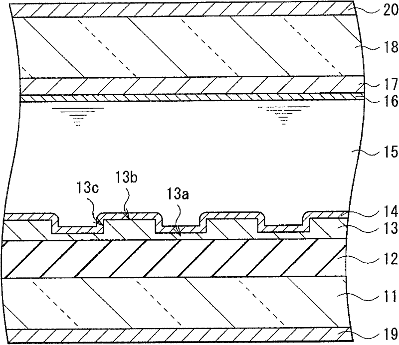
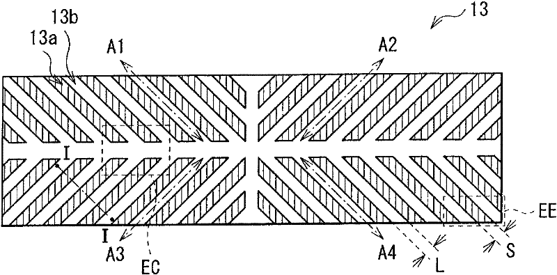
[0179] As a second example, the transmittance was measured with the slope angle θt of the slope 23 c in the pixel electrode 23 described in Modification 3 varied. Specifically, such as Figure 38 As shown, the inclination angle θt of the slope is changed under the following conditions: the width S (4 μm) of the concave surface 23a, the thickness Ta (50nm), the pitch (=the width of the bottom of the trapezoidal convex surface: 4μm), and the thickness Tb (200nm) of the convex surface 23b are constant , while the width Da of the convex surface 23b varies. At this time, the width Da changes stepwise by 0.5 μm within the range of 3.5 μm to 1 μm (both inclusive). In either case, there is no problem with liquid crystal orientation, and if Figure 39 As shown, the transmittance is very high. Also, when the width Da is 1 μm, the transmittance is highest.


PUM

PropertyMeasurementUnit
thicknessaaaaaaaaaa
thicknessaaaaaaaaaa
thicknessaaaaaaaaaa

Abstract

The invention relates to a liquid crystal display and a method for manufacturing the liquid crystal display. The liquid crystal display comprises a liquid crystal layer, a first substrate and a second substrate. The first substrate and the second substrate are disposed opposite to each other and the liquid crystal layer is arranged therebetween. A plurality of pixel electrodes are arranged on the first substrate adjacent to the liquid crystal layer. A counter electrode is arranged on the second substrate facing the plurality of pixel electrodes. At least one of the surface of the liquid crystal layer of the pixel electrodes and the surface of the liquid crystal layer of the counter electrode is equipped with a concavo-convex structure. The liquid crystal display is good in voltage response characteristics and high in transmittance.

Description

[0001] Cross References to Related Applications [0002] This application contains information related to the disclosures of Japanese Priority Patent Application JP 2010-087658 filed with the Japan Patent Office on April 6, 2010 and Japanese Priority Patent Application JP 2011-038640 filed with the Japan Patent Office on February 24, 2011 subject matter, the entire contents of these two prior applications are hereby incorporated by reference. technical field [0003] The present invention relates to a liquid crystal display using, for example, a vertical alignment (VA) mode liquid crystal, and a method for manufacturing the liquid crystal display. Background technique [0004] In recent years, for example, a VA (Vertical Alignment) mode is used in a liquid crystal display (LCD) device. In a liquid crystal display, a liquid crystal layer with anisotropic refractive index is sealed between a substrate provided with a pixel electrode and a substrate provided with a counter ele...

Claims


Application Information

Patent Timeline
Patent Type & Authority Applications(China)
IPC IPC(8): G02F1/1343G02F1/1333
CPCG02B6/0046G02F1/133528G02F1/133753G02F1/13452G02F1/136286G02F1/1368
Inventor 仲村真彦诹访俊一宫川干司井上雄一矶崎忠昭长濑洋二
Owner SONY CORP
Why Eureka
Try Eureka