Scanning signal line driving circuit, shift register, and method of driving shift register

一种扫描信号线、移位寄存器的技术,应用在移位寄存器及其驱动领域

Active Publication Date: 2011-10-19
SHARP KK
View PDF4 Cites 13 Cited by
  • Summary
  • Abstract
  • Description
  • Claims
  • Application Information

AI Technical Summary

Problems solved by technology

However, due to the influence of parasitic capacitance formed in the circuit constituting the shift register, the potential of the scanning signal may fluctuate from a low-level potential to a positive direction during the non-selection period.

Method used


Image

  • Scanning signal line driving circuit, shift register, and method of driving shift register
  • Scanning signal line driving circuit, shift register, and method of driving shift register
  • Scanning signal line driving circuit, shift register, and method of driving shift register

Examples


Embodiment Construction

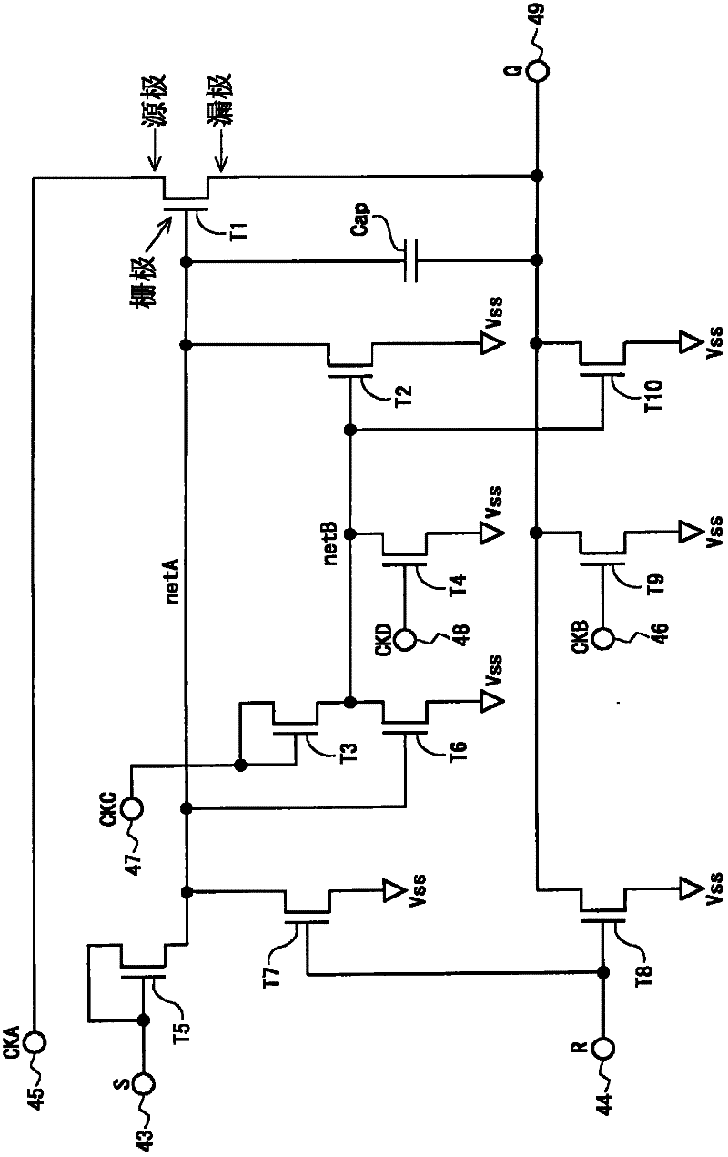
[0186] Hereinafter, an embodiment of the present invention will be described with reference to the drawings. In addition, in the following description, the gate terminal (gate electrode) of the thin film transistor corresponds to the first electrode, the source terminal (source electrode) corresponds to the second electrode, and the drain terminal (drain electrode) corresponds to the second electrode. 3 electrodes.

[0187]

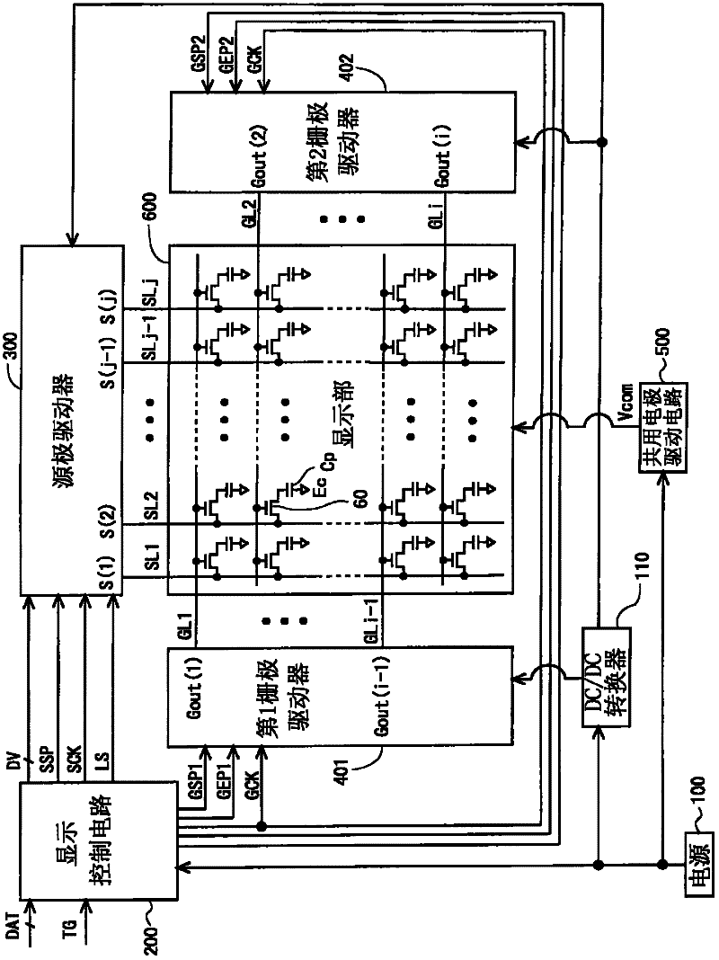
[0188] figure 2 It is a block diagram showing the overall configuration of an active matrix liquid crystal display device according to an embodiment of the present invention. like figure 2 As shown, the liquid crystal display device includes a power supply 100, a DC / DC converter 110, a display control circuit 200, a source driver (video signal line driving circuit) 300, a first gate driver (first scanning signal line driving circuit) 401 , a second gate driver (second scanning signal line driver circuit) 402 , a common electrode driver circuit 500 ...


PUM


Abstract

Provided is a scanning signal line driving circuit (for a display device) capable of suppressing unnecessary power consumption due to a leak current in a thin film transistor even in a case where a circuit in a shift register uses the thin film transistor having a relatively large off-leak current. Each bistable circuit constituting the shift register comprises a thin film transistor (T1) for increasing the potential of an output terminal (49) on the basis of a first clock, a region (netA) connected to the gate terminal of the thin film transistor (T1), a thin film transistor (T2) for reducing the potential of the region (netA), and a region (netB) connected to the gate terminal of the thin film transistor (T2). In such a configuration, the potential of the region (netB) is increased on the basis of a third clock having a phase ahead of that of the first clock by 90 degrees and is reduced on the basis of a fourth clock having a phase behind that of the first clock by 90 degrees.

Description

technical field [0001] The present invention relates to a driving circuit and a driving method of an active matrix display device, in particular to a shift register and a shift register in a scanning signal line driving circuit for driving a scanning signal line provided in a display portion of an active matrix display device. drive method. Background technique [0002] Liquid crystal display devices using amorphous silicon (a-Si) thin film transistors (hereinafter referred to as "a-SiTFT") as drive elements have been known in the past. In recent years, microcrystalline silicon (μc- Si) thin film transistor (hereinafter referred to as "μc-SiTFT") is developed as a liquid crystal display device used as a driving element. The mobility of microcrystalline silicon is higher than that of amorphous silicon, and μc-SiTFT is formed in the same process as that of a-SiTFT. Therefore, the use of μc-SiTFT as a driving element is expected to reduce the frame area, reduce the number of ...

Claims


Application Information

Patent Timeline
Patent Type & Authority Applications(China)
IPC IPC(8): G09G3/36G02F1/133G09G3/20
CPCG09G3/3677G09G2310/0286G09G2330/021G09G2330/025G11C19/184G11C19/28
Inventor 岩濑泰章坂本真由子
Owner SHARP KK
Why Eureka
Try Eureka