Cleaning process cavity and cleaning process for semiconductor silicon slice

A technology for process chambers and semiconductors, applied in liquid cleaning methods, semiconductor/solid-state device manufacturing, cleaning methods and appliances, etc., can solve the problems of low utilization rate of process chamber equipment, inoperable process chambers, and reduced equipment utilization. , to achieve the effect of improving equipment utilization, shortening cleaning time and saving time

Active Publication Date: 2011-11-16
SHANGHAI INTEGRATED CIRCUIT RES & DEV CENT
View PDF5 Cites 5 Cited by
  • Summary
  • Abstract
  • Description
  • Claims
  • Application Information

AI Technical Summary

Problems solved by technology

[0005] However, during the operation of the equipment, when the external mechanical arm places and takes out the silicon wafers from the process chamber, the process chamber cannot work, and it is necessary to wait until the silicon wafers are transported before cleaning, which greatly reduces the utilization rate of the equipment. Lower equipment utilization for process chambers that can clean multiple wafers at the same time

Method used


Image

  • Cleaning process cavity and cleaning process for semiconductor silicon slice
  • Cleaning process cavity and cleaning process for semiconductor silicon slice
  • Cleaning process cavity and cleaning process for semiconductor silicon slice

Examples


Embodiment Construction

[0031] The cleaning process chamber for semiconductor silicon wafers and the cleaning process for semiconductor silicon wafers proposed by the present invention will be further described in detail below in conjunction with the accompanying drawings and specific embodiments. Advantages and features of the present invention will be apparent from the following description and claims. It should be noted that all the drawings are in very simplified form and use imprecise ratios, which are only used for the purpose of conveniently and clearly assisting in describing the embodiments of the present invention.

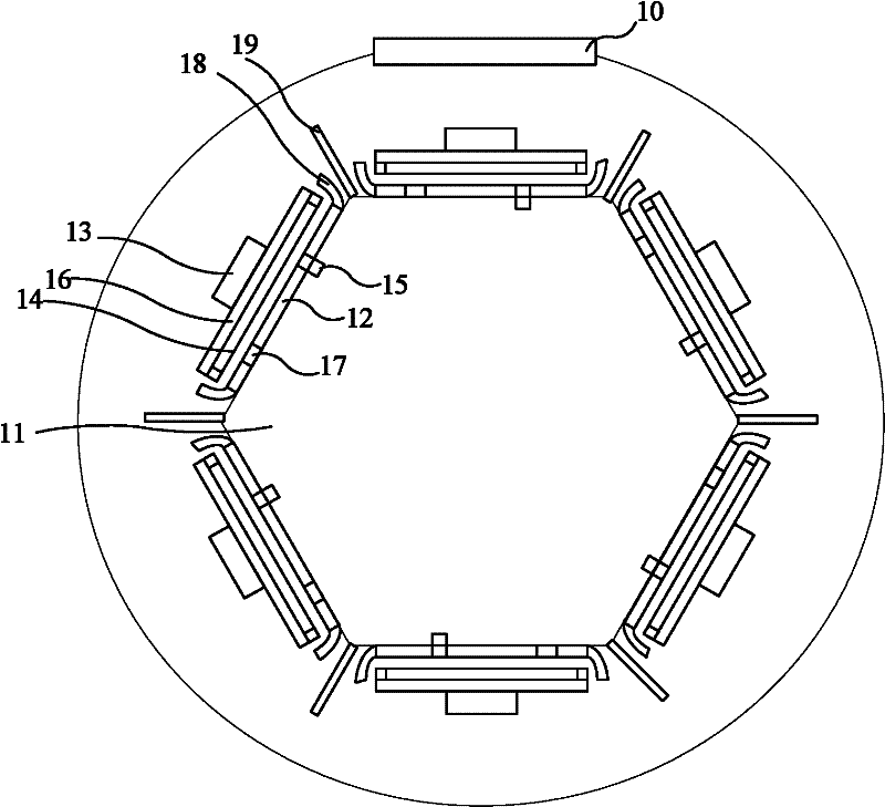
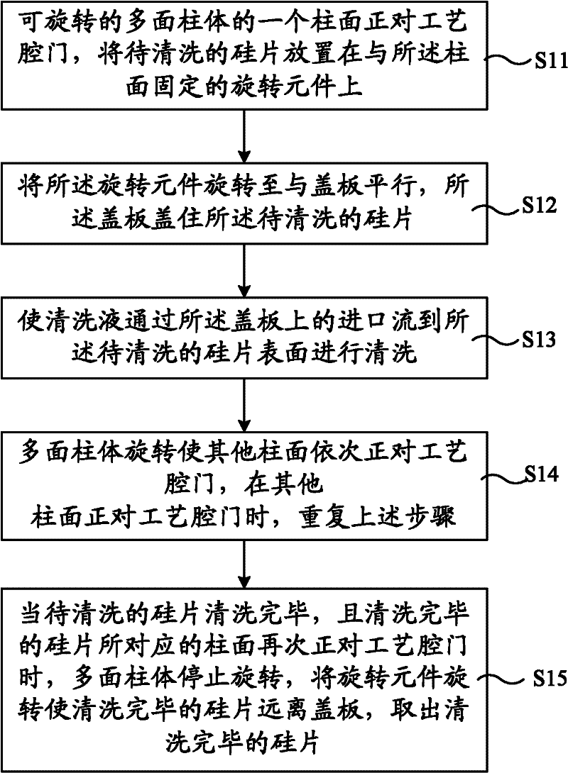
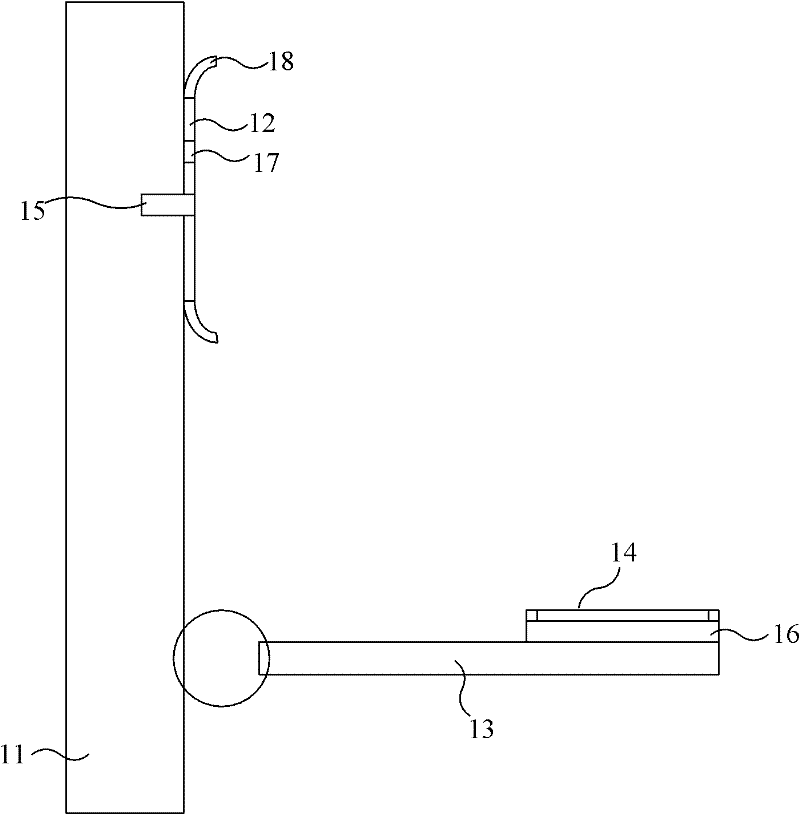
[0032] Please refer to figure 1 , figure 1 Shown is a schematic top view structural diagram of a semiconductor silicon wafer cleaning process chamber according to a preferred embodiment of the present invention. The invention provides a cleaning process chamber for semiconductor silicon wafers. The process chamber has a rotatable multi-faceted cylinder 11 inside, and a cover ...


PUM


Abstract

The invention provides a cleaning process cavity for a semiconductor silicon slice. A rotary polyhedral cylinder is arranged in the process cavity; each cylindrical surface is provided with a cover board; the cover boards are provided with one or more inlets; a rotary element is fixed on each cylindrical surface; silicon slices are arranged on the rotary elements; and the rotary elements can rotate to positions where the cover boards cover the silicon slices. The invention also provides a cleaning process for the semiconductor silicon slice. By use of the cleaning process cavity provided by the invention, when one silicon slice is put into and taken out of the process cavity through an outer manipulator, cleaning of other silicon slices can be performed normally; therefore, the equipment utilization rate is increased greatly and the time of cleaning the silicon slices is saved.

Description

technical field [0001] The invention relates to the technical field of integrated circuit technology, in particular to a cleaning process chamber for semiconductor silicon wafers and a cleaning process for semiconductor silicon wafers. Background technique [0002] With the continuous progress of integrated circuit manufacturing technology, the volume of semiconductor devices is becoming smaller and smaller, which also leads to very small particles becoming enough to affect the manufacturing and performance of semiconductor devices, so the silicon wafer cleaning process has also become more and more important. [0003] At present, the cleaning method widely used in the industry is wet cleaning, that is, various chemical solutions and pure water are used to clean silicon wafers. When the chemical solution contacts the silicon wafer, there is a very thin water film on the surface of the silicon wafer. Due to the effect of intermolecular attraction, this layer of water film is...

Claims


Application Information

Patent Timeline
Patent Type & Authority Applications(China)
IPC IPC(8): H01L21/00H01L21/02B08B3/12
Inventor 张晨骋
Owner SHANGHAI INTEGRATED CIRCUIT RES & DEV CENT
Why Eureka
Try Eureka