Eureka AIR delivers breakthrough ideas for toughest innovation challenges, trusted by R&D personnel around the world.

Scanning configuration of two-dimensional capacitance sensor and positioning method

A technology of electrodes and touch electrodes, which is applied in the field of scanning configuration and positioning of two-dimensional capacitive sensors, can solve problems such as misjudgment, unstable data, and poor anti-interference performance, and achieve the effect of enhancing anti-interference and restraining interference

Inactive Publication Date: 2011-11-23
SUZHOU PIXCIR MICROELECTRONICS
View PDF2 Cites 8 Cited by
  • Summary
  • Abstract
  • Description
  • Claims
  • Application Information

AI Technical Summary

Problems solved by technology

[0003] The above-mentioned row-by-row or column-by-column scanning configuration method, although the scanning method is relatively simple, but because there are differences in external interference in different time periods, the detected data is not very stable, which eventually leads to possible touch operations. It is regarded as not touched, but not touched is regarded as touched, and it cannot be accurately judged whether it is touched. When the external interference is more serious, it may even detect that the coordinates drift relative to the touched point. The above will directly lead to poor anti-interference performance and error. Judgment

Method used

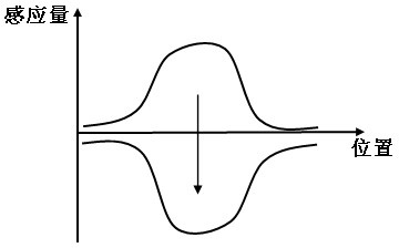
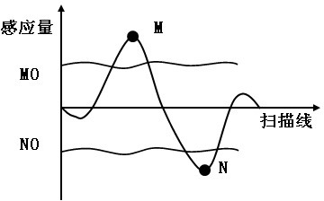

Image

  • Scanning configuration of two-dimensional capacitance sensor and positioning method
  • Scanning configuration of two-dimensional capacitance sensor and positioning method
  • Scanning configuration of two-dimensional capacitance sensor and positioning method

Examples


Embodiment Construction

[0012] The present invention will be further described below in conjunction with the accompanying drawings and embodiments.

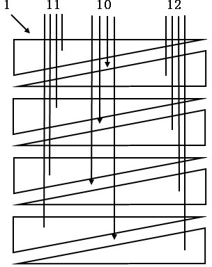
[0013] The scanning configuration of the two-dimensional capacitive sensor involved in the present invention has a single-layer electrode group arranged on one side, that is, a single-layer electrode, please refer to figure 1 As shown in the wiring structure of the electrode layer 1, the electrode layer 1 is composed of a plurality of electrode groups 10, and each electrode group 10 has two touch electrodes, namely positive touch electrodes 11 and negative touch electrodes 12. The positive touch electrodes 11 and the negative touch electrodes 12 are arranged opposite to each other, and the electrodes in one direction are respectively arranged in the gap area between the electrodes in the other direction.

[0014] In the present invention, when scanning the electrode layer 1 row by row or column by row, two rows or two columns are scanned at the same ti...


PUM


Abstract

The invention relates to a scanning configuration of a two-dimensional capacitance sensor and a positioning method. The scanning configuration has a single layer of electrode groups arranged on one side, wherein each electrode group comprises two touch electrodes, namely a positive touch electrode and a negative touch electrode; and during scanning, one touch electrode in each electrode group serves as a scanning end, and the other touch electrode serves as a reference end. The invention has the advantages that: the scanning configuration and the positioning method are simple; interference caused by outside noises can be effectively prevented; and interference resistance is improved, so coordinates of specific positions of touch points can be quickly and accurately found.

Description

technical field [0001] The invention relates to a scanning configuration of a sensor, in particular to a scanning configuration and a positioning method of a two-dimensional capacitive sensor. Background technique [0002] The so-called two-dimensional capacitive sensor refers to a device or device that uses the principle of capacitance to transmit signals in the X and Y directions. It can be an ITO (indium tin oxide) layer, a PCB board, a keyboard or a touch screen, etc., usually by human fingers. Or stylus actuation. In order to detect the specific position where the touch object touches the touch screen, in the existing scanning configuration of the two-digit capacitive sensor, it generally scans in a row-by-row or column-by-column manner, that is, scans one row or one column at each moment. In order to characterize the change in capacitance before and after touch, it is necessary to linearly convert the capacitance value of the scanning row or column into a quantity tha...

Claims


Application Information

Patent Timeline
IPC IPC(8): G06F3/041G06F3/044
Inventor 雷奥纳·波特曼
Owner SUZHOU PIXCIR MICROELECTRONICS
Why Eureka
Eureka Blog
Learn More