

Pixel structure of organic light emitting diode (OLED)
A technology of light-emitting display and pixel structure, applied in the field of pixel structure, can solve the problems of affecting the resolution and reducing the organic light-emitting display, and achieve the effect of increasing the resolution and the aperture ratio
- Summary
- Abstract
- Description
- Claims
- Application Information
AI Technical Summary
Problems solved by technology
Method used
Image

Examples
Embodiment Construction
[0013] The specific implementation manners of the present invention will be described in further detail below with reference to the accompanying drawings.
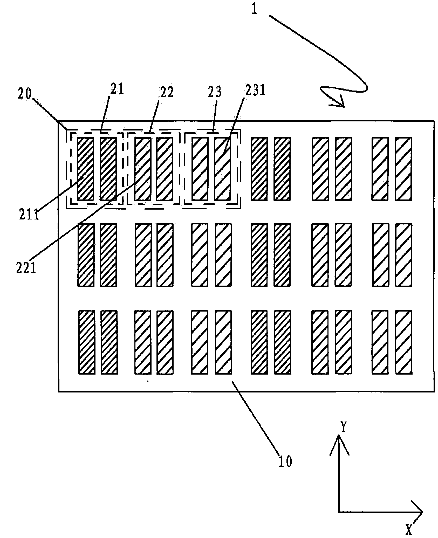
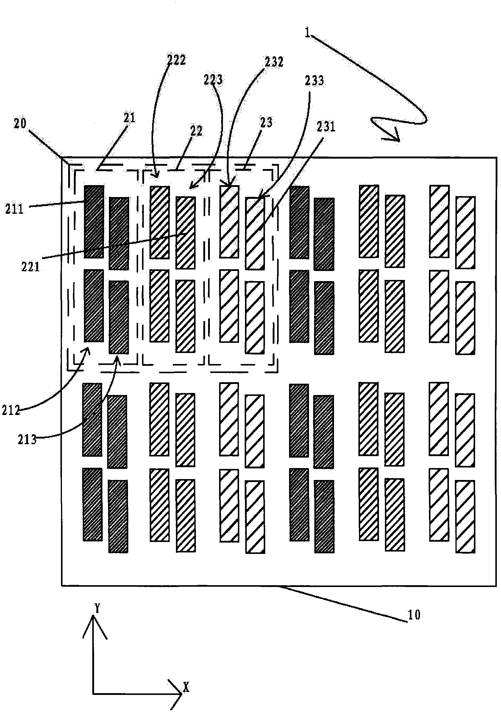
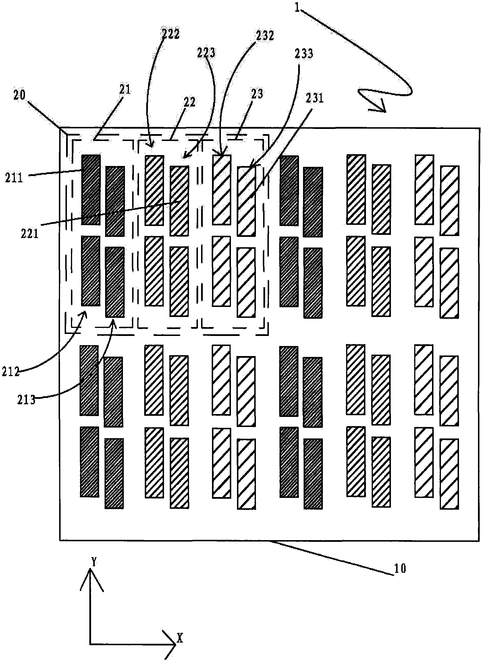
[0014] figure 1 A schematic structural diagram of a pixel structure of an organic light emitting display according to an embodiment of the present invention is shown. refer to figure 1 , the pixel structure 1 is located on the substrate 10, including a plurality of pixels 20, each pixel 20 has a first sub-pixel unit 21, a second sub-pixel unit 22 and a third sub-pixel unit 23 in the direction of the X-axis, the first sub-pixel unit The pixel unit 21 has two red (R) sub-pixels 211 , the second sub-pixel unit 22 has two green (G) sub-pixels 221 , and the third sub-pixel unit 23 has two blue (B) sub-pixels 231 . Therefore, if figure 1 As shown, the red, green and blue sub-pixels in the pixel structure 1 are repeatedly arranged in this order in the X-axis direction: red (R), red (R), green (G), green (G), blue (B), blue (B...
PUM
 Abstract
Description
Claims
Application Information