Method for testing high-voltage MOS device

A technology of MOS devices and testing methods, which is applied in the direction of single semiconductor device testing, semiconductor/solid-state device testing/measurement, etc., can solve problems such as inaccurate source-drain current testing, and achieve the effect of avoiding too small source-drain current

Inactive Publication Date: 2012-03-21
SHANGHAI HUAHONG GRACE SEMICON MFG CORP
View PDF1 Cites 27 Cited by
  • Summary
  • Abstract
  • Description
  • Claims
  • Application Information

AI Technical Summary

Problems solved by technology

[0006] The purpose of the present invention is to provide a test method for high-voltage MOS devices, which can effectively solve the problem of inaccurate testing caused by premature saturation of source and drain currents

Method used


Image

  • Method for testing high-voltage MOS device
  • Method for testing high-voltage MOS device
  • Method for testing high-voltage MOS device

Examples


Embodiment Construction

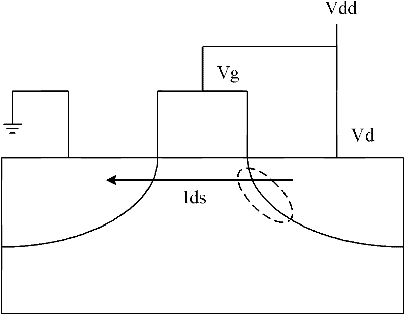
[0024] As can be seen from the background technology section, the existing high-voltage MOS device testing method applies a fixed test voltage to the gate and source to test the source-drain current flowing through, which is likely to affect the parasitic effect of the MOS device due to the parasitic effect caused by the high voltage. Electrical performance, resulting in inaccurate testing.

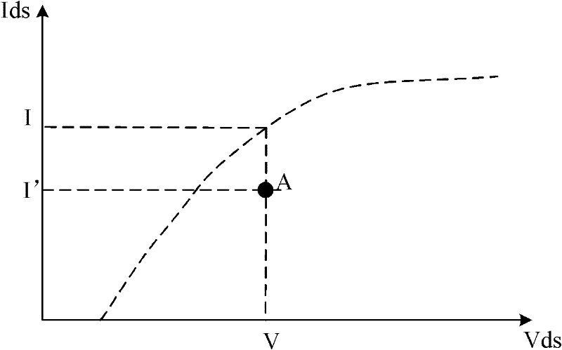
[0025] figure 2 The output characteristic curve of the transistor using the existing test method is shown. like figure 2 As shown, it is assumed that under normal circumstances, the output characteristic curve of the high-voltage MOS device should be a dotted line (because the gate is usually connected to the drain during testing, the high-voltage MOS device is not turned on at the beginning of the characteristic curve, and the source-drain current is 0). The critical voltage value of its saturation region is V, and the saturation current is I. And if the test voltage is suddenly ap...


PUM


Abstract

The utility model provides a method for testing a high-voltage MOS (Metal Oxide Semiconductor) device. The method is used for testing whether the high-voltage MOS device of each chip on a semiconductor wafer becomes invalid, and comprises the following steps of: optionally selecting a plurality of chips on the semiconductor wafer and testing the high-voltage MOS devices thereof; grounding one pole of the high-voltage MOS device of each chip and connecting the other pole and the gate thereof to a test end; gradually increasing a test voltage applied to the test end, and simultaneously measuring the corresponding source-drain current of each high-voltage MOS device, wherein the initial value of the test voltage is lower than the saturation voltage of the high-voltage MOS device; forming the output characteristic curve of the high-voltage MOS device of each chip according to the test voltage and the corresponding source-drain current; and determining whether the high-voltage MOS device becomes invalid according to the output characteristic curve. Compared with the prior art, the method is to test the source-drain currents by gradually increasing and adjusting the test voltage, so that the problem of wrong determination due to low source-drain currents caused by the parasitic effect can be avoided.

Description

technical field [0001] The invention relates to the field of semiconductor device testing, in particular to a testing method for a high-voltage MOS device (HVMOS). Background technique [0002] At the back end of the semiconductor manufacturing process, functional testing of chips on semiconductor wafers is often required. A well-tested wafer can be put into subsequent use as an effective product. With the increasing size of the wafer, the number of chips on a single wafer is also increasing. It is impossible to test the device functions of all chips one by one. Only a few points on the wafer are randomly selected to test their device functions. [0003] In recent years, high-voltage MOS devices (HV MOS) have been widely used, such as power supply control, driving circuits and other fields. Its operating voltage is tens of volts or even hundreds of volts. Many physical characteristics brought by high voltage, especially the reliability of high-voltage MOS devices, are the ...

Claims


Application Information

Patent Timeline
Patent Type & Authority Applications(China)
IPC IPC(8): G01R31/26H01L21/66
Inventor 韦敏侠
Owner SHANGHAI HUAHONG GRACE SEMICON MFG CORP
Why Eureka
Try Eureka