
Structure of semiconductor device

A device structure, semiconductor technology, applied in the direction of semiconductor devices, semiconductor/solid-state device components, semiconductor/solid-state device testing/measurement, etc., can solve the problem of easy to burn test structures

Active Publication Date: 2013-10-30
SEMICON MFG INT (SHANGHAI) CORP +1
View PDF4 Cites 0 Cited by
  • Summary
  • Abstract
  • Description
  • Claims
  • Application Information

AI Technical Summary

Problems solved by technology

However, this analysis method uses the method of applying electrical signals, so the current / voltage is too large and it is easy to burn the test structure

Method used


Image

  • Structure of semiconductor device
  • Structure of semiconductor device
  • Structure of semiconductor device

Examples


Embodiment 1

[0051] Firstly, the layer is peeled to expose the first dielectric layer where the finger structure 300 is located;

[0052] Such as Figure 3A As shown, one end 301a of the serpentine metal wire 301 is grounded, and a double-beam microscope is used to conduct PVC analysis on the test structure, and the voltage and contrast of the double-beam microscope are adjusted. At this time, the serpentine metal wire 301 is partially bright and partially dark. , the light-dark junction is the open circuit failure position 301b;

[0053] If there is a short circuit between the ground end 301a of the serpentine metal wire and the broken circuit failure position 301b and the finger structure 300a, that is, there is a short circuit between the highlighted section of the serpentine metal wire 301 and the finger structure 300, then The short-circuit failure finger structure 300a will show a highlighted state, so that the short-circuit failure position can be located to a specific finger struc...

Embodiment 2

[0059] First, peeling off the semiconductor device sample to expose the first dielectric layer;

[0060] Such as Figure 4A As shown, any end 401a of the serpentine metal wire 401 is grounded, and a double-beam microscope is used to conduct PVC analysis on the test structure, and the voltage and contrast of the double-beam microscope are adjusted. At this time, it can be observed that the serpentine metal wire 401 is partially highlighted, Partially dark state, then the light-dark junction is the open circuit failure position 401b;

[0061] Such as Figure 4B As shown, choose to ground the open circuit failure position 401b or the ungrounded end 401c of the serpentine metal wire 401, if the ungrounded end 401c of the serpentine metal wire 401 is grounded, then use a double-beam microscope to perform PVC analysis on the test structure , adjust the voltage and contrast of the double-beam microscope. At this time, it can be observed that the part from the broken circuit failure...


PUM


Abstract

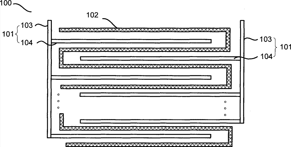
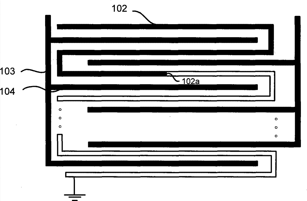
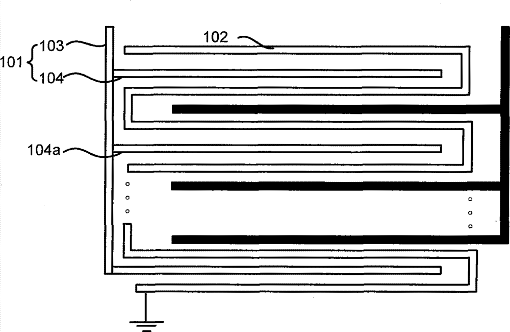
The invention relates to the structure of a semiconductor device, which comprises a metal interconnection line to be tested and a test structure for analyzing the short circuit and open circuit invalidation of the metal interconnection line to be tested, wherein the test structure comprises two comb-shaped structures and an snake-shaped metal wire, two finger-shaped structures which respectively belong to the two comb-shaped structures, the snake-shaped metal wire and the metal interconnection line to be tested are arranged in the same plane, and the finger-shaped structures are connected with two handle parts by a plurality of through holes which are filled with conductive materials. When the short circuit and open circuit invalidation position of the test structure is positioned, the handle parts are firstly removed in a peeling way, the same group of finger-shaped structures is disconnected from one another, the test structure is subject to poly vinyl chloride (PVC) analysis by a double beam microscope, and only the finger-shaped structure which is in short circuit with the snake-shaped metal wire is high in luminance, so that the short circuit invalidation position can be immediately positioned at one specific finger-shaped structure, and the efficiency of invalidation analysis can be improved.

Description

technical field [0001] The invention relates to a semiconductor manufacturing process, in particular to a semiconductor device structure with a failure analysis test structure. Background technique [0002] In the large-scale production of semiconductor devices, through failure analysis (Failure Analysis FA) of semiconductor devices after design and manufacture, defects can be found and corrected to solve the problems caused by defects. Therefore, failure analysis of semiconductor devices is very important for improving yield , It is very important to improve the reliability and stability of the process technology. [0003] As the integration level of integrated circuits continues to increase, the metal interconnection lines become thinner, narrower, and thinner, so the current density in them is increasing. Under the action of higher current density, the metal atoms in the metal interconnection will migrate along the direction of electron movement, and this phenomenon is c...

Claims


Application Information

Patent Timeline
Patent Type & Authority Patents(China)
IPC IPC(8): H01L23/544H01L21/66G01R31/02
Inventor 梁山安务林凤郭强
Owner SEMICON MFG INT (SHANGHAI) CORP
Learn More