
Method for testing blocking capacity of photoresist layer to ion implantation

A technology of injecting blocking and photoresist glue, which is applied in semiconductor/solid-state device testing/measurement, electrical components, semiconductor/solid-state device manufacturing, etc. It can solve the problems of costing test wafers, missing, and discontinuous thickness of photoresist glue layer, etc. Achieve the effect of reducing test cost and reducing the number of wafers

Inactive Publication Date: 2012-04-04
SEMICON MFG INT (SHANGHAI) CORP +1
View PDF4 Cites 11 Cited by
  • Summary
  • Abstract
  • Description
  • Claims
  • Application Information

AI Technical Summary

Benefits of technology

This technology uses an equal-thickness photo resist film onto a silicon substrate surface. By adjusting how fast it rotates at certain speeds, we get thin layers along its edges rather than just being applied over all areas equally. These films are tested separately until they meet specific conditions where there will cause damage during ion beam treatment (IB). To reduce costs while optimizing performance, this process involves applying several coatings of varying sizes across both sides of the Si chip's surface.

Problems solved by technology

This patented describes methods used to measure how well a specific material called silicone reservoirs or photo resist blocks impurity ions like dopants during ion-implanted processing operations. However, current techniques require manual adjustment of the materials' properties before performing tests, making them time-consuming and prone to errors due to human error.

Method used


Image

  • Method for testing blocking capacity of photoresist layer to ion implantation
  • Method for testing blocking capacity of photoresist layer to ion implantation
  • Method for testing blocking capacity of photoresist layer to ion implantation

Examples


Embodiment Construction

[0023] In order to make the object, technical solution, and advantages of the present invention clearer, the present invention will be further described in detail below with reference to the accompanying drawings and examples.

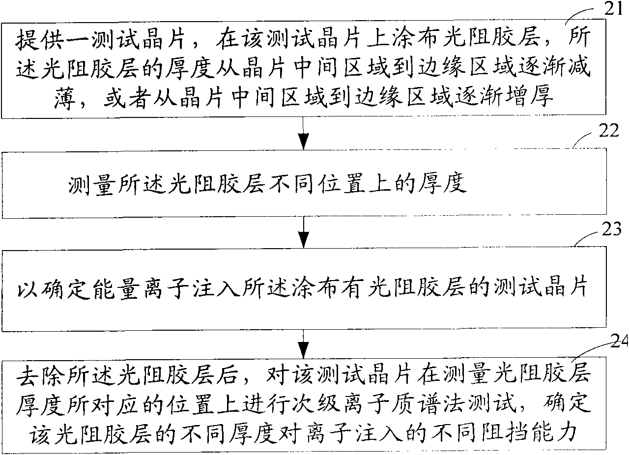
[0024] The invention provides a method for testing the blocking ability of the photoresist adhesive layer to ion implantation, the schematic flow chart of which is as follows figure 1 As shown, the method includes:

[0025] Step 21, providing a test wafer, coating a photoresist layer on the test wafer, the thickness of the photoresist layer gradually decreases from the middle area of ​​the wafer to the edge area, or gradually increases from the middle area to the edge area of ​​the wafer .

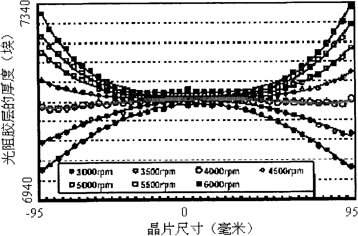
[0026] The coating of the photoresist layer in this step is realized by controlling the rotation speed of the wafer. Because when coating the photoresist glue layer on the surface of the wafer, at first it is necessary to drop the solvent of the photoresist glue ...


PUM


Abstract

The invention provides a method for testing blocking capacity of a photoresist layer to ion implantation, which includes firstly, providing a testing wafer coated with a photoresist layer, wherein the photoresist layer is thinned gradually from the middle region of the wafer to the edge region of the wafer or thickened gradually from the middle region of the wafer to the edge region of the wafer, secondly, measuring thicknesses of different positions of the photoresist layer, thirdly, determining energy ions to be implanted into the testing wafer coated with the photoresist layer, and fourthly, removing the photoresist layer and testing at positions corresponding to photoresist layer thickness measuring positions of the testing wafer by means of secondary ion mass spectrometry to determine different blocking capacities of different thicknesses of the photoresist layer to ion implantation. Using the method for testing blocking capacity of the photoresist layer to ion implantation can effectively reduce testing cost.

Description


Claims


Application Information

Patent Timeline
Owner SEMICON MFG INT (SHANGHAI) CORP
Learn More