Supercharge Your Innovation With Domain-Expert AI Agents!

Ultralow capacitance transient voltage suppression device and manufacturing method thereof

A technology of transient voltage suppression and manufacturing methods, which is applied in semiconductor/solid-state device manufacturing, electric solid-state devices, electrical components, etc., can solve the problems of device performance impact and high cost, and achieve high performance and low cost

Active Publication Date: 2014-02-26
HANGZHOU SILAN INTEGRATED CIRCUIT +1
View PDF7 Cites 0 Cited by
  • Summary
  • Abstract
  • Description
  • Claims
  • Application Information

AI Technical Summary

Problems solved by technology

[0014] Due to the silicon integration process and the yield rate, the ultra-low capacitance TVS devices formed by the above-mentioned combination are all in the form of separate device combination packaging, that is, the upper and lower diodes 11, 12 and TVS tube 13 are all obtained through different layouts and processes. To achieve, and then combined together through packaging, this technology is not only costly, but also the performance of the device will be affected by the properties of the connecting wire material

Method used


Image

  • Ultralow capacitance transient voltage suppression device and manufacturing method thereof
  • Ultralow capacitance transient voltage suppression device and manufacturing method thereof
  • Ultralow capacitance transient voltage suppression device and manufacturing method thereof

Examples


Embodiment Construction

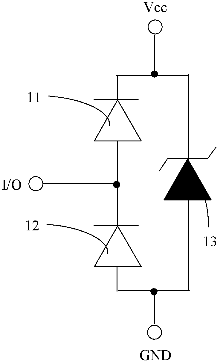
[0067] In the prior art, the upper diode, the lower diode and the TVS tube in the ultra-low capacitance TVS device all use discrete devices, the cost is high, and the performance is affected by the properties of the connecting wire material.

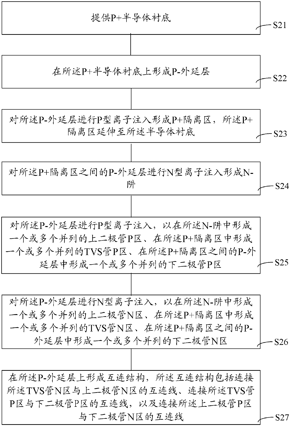
[0068] In the ultra-low-capacity transient voltage suppression device and its forming method according to the embodiment of the present invention, the upper diode, the lower diode and the TVS tube are all integrated on the same P+ semiconductor substrate, which is beneficial to realize low cost and high performance.

[0069] In addition, in this embodiment, the P+ isolation region extends to contact with the P+ semiconductor substrate, so that the P+ semiconductor substrate can be used as the ground GND electrode, and there is no need to lead the electrode from the front side, which is not only beneficial to reducing the chip size, but also applicable to A variety of different packaging forms, in addition, the P+ semiconductor substrate i...


PUM


Abstract

The invention provides an ultralow capacitance transient voltage suppression (TVS) device and a manufacturing method thereof. The ultralow capacitance transient voltage suppression device comprises a P+ semiconductor substrate, P- epitaxial layers which are positioned on the P+ semiconductor substrate, P+ isolation regions which are formed in the P- epitaxial layer and extend to the P+ semiconductor substrate, TVS tube N regions which are positioned in the P+ isolation regions, TVS tube P regions which are abreast with the TVS tube N regions and positioned in the P+ isolation regions, N- traps which are positioned in the P- epitaxial layers among the P+ isolation regions, upper diode P regions which are positioned in the N- traps, upper diode N regions which are abreast with the upper diode P regions and positioned in the N- traps, lower diode N regions which are positioned in the P- epitaxial layers among the P+ isolation regions, lower diode P regions which are abreast with the lower diode N regions and positioned in the P- epitaxial layers, and an interconnection structure which is positioned on the P- epitaxial layers. In the ultralow capacitance TVS device, upper diodes, lower diodes and TVS tubes are integrated on the same chip, so that low cost and high performance are realized.

Description

technical field [0001] The invention relates to the technical field of semiconductor devices and semiconductor technology, in particular to an ultra-low capacitance transient voltage suppression device and a manufacturing method thereof. Background technique [0002] Transient voltage suppressor diode (TVS, Transient Voltage Suppressor), also known as clamping diode, is a high-efficiency circuit protection device commonly used at present. Its shape is the same as that of ordinary diodes, but it can absorb surge power up to several thousand watts. , its main feature is that under reverse application conditions, when it is subjected to a high-energy large pulse, its working impedance will immediately drop to an extremely low conduction value, thereby allowing a large current to pass, while clamping the voltage at a predetermined level, generally The response time is only 10 -12 seconds, so it can effectively protect the precision components in the electronic circuit from bein...

Claims


Application Information

Patent Timeline
Patent Type & Authority Patents(China)
IPC IPC(8): H01L27/08H01L21/822
Inventor 张常军李昕华陈向东
Owner HANGZHOU SILAN INTEGRATED CIRCUIT
Features
  • R&D
  • Intellectual Property
  • Life Sciences
  • Materials
  • Tech Scout
  • Unparalleled Data Quality
  • Higher Quality Content
  • 60% Fewer Hallucinations
Learn More