Manufacture process of removing redundant metal filling of metal layer

A technology of redundant metal, manufacturing process, used in semiconductor/solid-state device manufacturing, electrical components, circuits, etc.

Inactive Publication Date: 2012-05-09
SHANGHAI HUALI MICROELECTRONICS CORP
View PDF7 Cites 9 Cited by
  • Summary
  • Abstract
  • Description
  • Claims
  • Application Information

AI Technical Summary

Problems solved by technology

Redundant metal improves the uniformity of pattern density, but inevitably introduces additional coupling capacitance between metals

Method used


Image

  • Manufacture process of removing redundant metal filling of metal layer
  • Manufacture process of removing redundant metal filling of metal layer
  • Manufacture process of removing redundant metal filling of metal layer

Examples


Embodiment Construction

[0040] In order to further explain the technical means and effects of the present invention to achieve the intended purpose of the invention, the manufacturing process for removing redundant metal filling in the metal layer according to the present invention will be described in detail below in conjunction with the accompanying drawings and preferred embodiments.

[0041] Different embodiments of the present invention will be described in detail below to implement different technical features of the present invention. It should be understood that the units and configurations of the specific embodiments described below are used to simplify the present invention, which are only examples and not limiting scope of the invention.

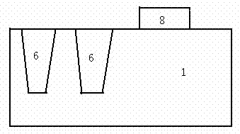
[0042] The present invention proposes a manufacturing process for removing redundant metal filling of metal layers, the process steps of which are as follows:

[0043] 1) Depositing a low-k dielectric layer;

[0044] 2) forming a hard mask layer on the ...


PUM

PropertyMeasurementUnit
thicknessaaaaaaaaaa

Abstract

The invention provides a manufacture process of removing redundant metal filling of a metal layer. The manufacture process comprises the following steps of: 1, depositing a low k value dielectric layer; 2, forming a hard mask layer on the deposited low k value dielectric layer; 3, photoetching and etching the hard mask layer; 4, completing photoetching and etching to form a through hole; 5, carrying out filling of a lead metal, a through hole metal and a redundant metal for completing metal layer deposition; 6, carrying out chemically mechanical polishing on the metal layer; and 7, continuously chemically mechanical polishing of the low k value dielectric layer and a metal hybrid layer, and further removing redundant metal. Through a process of further removing the redundant metal by using chemically mechanical polishing in the manufacture process of single- damascene and dual- damascene metal interconnections, a coupling capacitance introduced in the metal layers and among the metal layers by the redundant metal filling can be effectively reduced or eliminated, thus the manufacture process is very practical.

Description

technical field [0001] The invention relates to a semiconductor manufacturing process, in particular to a manufacturing process for removing redundant metal filling in a metal layer. Background technique [0002] As the integration level of semiconductor chips continues to increase, the feature size of transistors continues to shrink. After entering the 130nm technology node, limited by the high resistance characteristics of aluminum, copper interconnection gradually replaces aluminum interconnection and becomes the mainstream of metal interconnection. Since the copper dry etching process is not easy to realize, the manufacturing method of the copper wire cannot be obtained by etching the metal layer like the aluminum wire. The widely used manufacturing method of copper wire is damascene technology called damascene process. In this process, a low-k dielectric layer is first deposited on the silicon wafer, and then a metal wire groove is formed in the dielectric layer by ph...

Claims


Application Information

Patent Timeline
Patent Type & Authority Applications(China)
IPC IPC(8): H01L21/768H01L21/321
Inventor 毛智彪胡友存戴韫青王剑
Owner SHANGHAI HUALI MICROELECTRONICS CORP
Why Eureka
Try Eureka