Supercharge Your Innovation With Domain-Expert AI Agents!

Semiconductor device structure and method for manufacturing same

A device structure and semiconductor technology, which is applied in the direction of semiconductor devices, semiconductor/solid-state device manufacturing, electrical components, etc., can solve the problems of lateral and vertical diffusion semiconductor device electrical characteristics deterioration, etc., to improve the SCE effect, improve the overall electrical performance, The effect of saving manufacturing cost

Active Publication Date: 2012-07-04
SEMICON MFG INT (SHANGHAI) CORP +1
View PDF8 Cites 0 Cited by
  • Summary
  • Abstract
  • Description
  • Claims
  • Application Information

AI Technical Summary

Problems solved by technology

[0004] It is not difficult to understand from the above description that although the ultra-shallow abrupt junction process can improve the SCE effect, if the lateral and vertical diffusion of impurities cannot be effectively controlled, the electrical characteristics of the semiconductor device may be deteriorated. For the two-step S / D This is especially true for injected NMOS transistors

Method used


Image

  • Semiconductor device structure and method for manufacturing same
  • Semiconductor device structure and method for manufacturing same
  • Semiconductor device structure and method for manufacturing same

Examples


no. 1 example

[0035] Below, will combine Figure 1A to Figure 1E , figure 2 as well as image 3 A method for fabricating a semiconductor device structure according to a first embodiment of the present invention will be described in detail.

[0036] Please refer to Figure 1A to Figure 1E , which shows schematic cross-sectional views of method steps for fabricating a semiconductor device structure according to a first embodiment of the present invention.

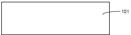
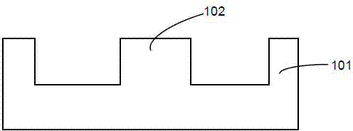
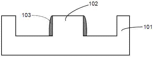
[0037] First, if Figure 1A As shown, a front-end device structure is provided, and the front-end device structure includes a semiconductor substrate 101 .

[0038] Wherein, the material constituting the semiconductor substrate 101 may be undoped single crystal silicon, single crystal silicon doped with impurities, or silicon-on-insulator (SOI) or the like. As an example, in this embodiment, the semiconductor substrate 101 is made of undoped single crystal silicon material.

[0039] Here, it should be noted that the structures of the ...

no. 2 example

[0069] Next, the first embodiment and Figure 4 to Figure 6 A method for fabricating a semiconductor device structure according to a second embodiment of the present invention will be described in detail. In the second embodiment, only the lateral diffusion barrier wall is formed to prevent the lateral diffusion of impurities in the S / D region, which is mainly based on the consideration of the complexity of the process. Other than that, other process steps and process parameters are the same as those of the first embodiment. Therefore, descriptions of these same process steps as well as process parameters and the like will be omitted.

[0070] Please refer to Figure 4 , which shows a flow chart of a method for fabricating a semiconductor device structure according to a second embodiment of the present invention, which is used to briefly show the flow of the entire method.

[0071] First, in step S401, a front-end device structure is provided, and the front-end device struc...


PUM


Abstract

A method for manufacturing a semiconductor device structure includes: providing a front-end device structure which comprises a semiconductor substrate; etching the semiconductor substrate to form grooves in portions, about to form a source / drain region, of the semiconductor substrate, so that a dummy gate structure is formed on a portion between the grooves; forming transverse diffusion barrier walls on the semiconductor substrate, wherein the transverse diffusion barrier walls are positioned on two sides of the dummy gate structure and close to the dummy gate structure; and forming a substrate epitaxial layer on the surface of the semiconductor substrate and the surface of the dummy gate structure, and planarizing the substrate epitaxial layer. The method is capable of effectively suppressing transverse diffusion of impurities in the source / drain region and enables the transverse diffusion to be designed separately from longitudinal diffusion, so that SCE (short channel effect) and overrun of the S / D (source / drain) region of a semiconductor device can be improved, and further integral electric property of the semiconductor device is improved.

Description

technical field [0001] The present invention relates to a semiconductor manufacturing process, and in particular, to a semiconductor device structure and a manufacturing method thereof. Background technique [0002] For a long time, in the semiconductor manufacturing process, the size reduction of gate and channel has been limited by the development of source / drain (S / D) junction and gate dielectric. Although the lightly doped source-drain (LDD) process and high dielectric constant (high-k) materials have been adopted, the short-channel effect (hereinafter referred to as the SCE effect) still faces major challenges. The SCE effect leads to various secondary effects in transistors, such as carrier velocity saturation effect that affects carrier mobility, hot carrier effect (HCE) that shortens device lifetime, and leakage induced degradation that deteriorates subthreshold characteristics. Barrier lowering effect (DIBL), which leads to increased leakage current between source ...

Claims


Application Information

Patent Timeline
Patent Type & Authority Applications(China)
IPC IPC(8): H01L21/336H01L21/31H01L29/78H01L29/06
Inventor 赵猛
Owner SEMICON MFG INT (SHANGHAI) CORP
Features
  • R&D
  • Intellectual Property
  • Life Sciences
  • Materials
  • Tech Scout
  • Unparalleled Data Quality
  • Higher Quality Content
  • 60% Fewer Hallucinations
Learn More