Method of manufacturing printed circuit board

A printed circuit board, circuit layer technology, applied in the direction of printed circuit, printed circuit, printed circuit manufacturing, etc.

Inactive Publication Date: 2012-07-11
SAMSUNG ELECTRO MECHANICS CO LTD
View PDF5 Cites 3 Cited by
  • Summary
  • Abstract
  • Description
  • Claims
  • Application Information

AI Technical Summary

Problems solved by technology

However, the size of the land 43 usually occupies a considerable area of ​​the printed circuit board (seven or more times the upper area of ​​the via hole), so this becomes an obstacle to the realization of a high integration / high density printed circuit board.

Method used


Image

  • Method of manufacturing printed circuit board
  • Method of manufacturing printed circuit board
  • Method of manufacturing printed circuit board

Examples


Embodiment Construction

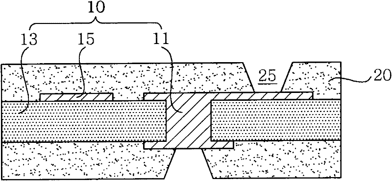
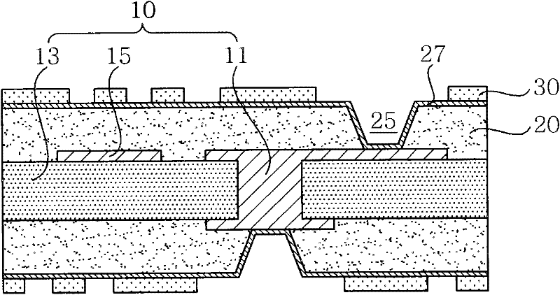
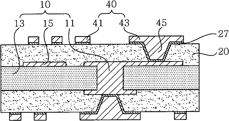
[0028] Embodiments of the present invention will be described in detail below in conjunction with the accompanying drawings, so as to more clearly understand the purpose, features and advantages of the present invention.

[0029] The terms and words used in the description and claims of the present invention should not be construed as limited to the usual meanings and dictionary definitions, but should be understood as based on the inventor's ability to properly define the concepts implied by the terms, to best To describe the principles of the method known to him or her to carry out the present invention, these terms and words should be understood as having meanings and concepts related to the technical scope of the present invention.

[0030] The above and other objects, features and advantages of the present invention can be more clearly understood through the following detailed description in conjunction with the accompanying drawings. In the specification, in adding refer...


PUM


Abstract

Disclosed herein is a method of manufacturing a printed circuit board that simultaneously forms a via and an embedding land and thus improves the matching value of the via and the embedding land to secure interlayer conduction reliability, and further simultaneously forms the via and the embedding land to reduce manufacturing costs. In addition, the embedding land is formed to be embedded in the second insulating layer to implement high-density / high-integration of the printed circuit board and a via is formed in less time as compared to a method of forming a via hole using laser to reduce a process time.

Description

[0001] Cross References to Related Applications [0002] This application claims priority to Korean Patent Application No. 10-2010-0131347, filed Dec. 21, 2010, entitled "Method Of Manufacturing Printed Circuit Board," which is hereby incorporated in its entirety Incorporated into this application by reference. technical field [0003] The invention relates to a method of manufacturing a printed circuit board. Background technique [0004] With the recent development of the electronics industry, there is an increasing demand for high performance and miniaturization of electronic devices. Therefore, research and development for realizing high-density circuit patterns on printed circuit boards on which electronic components are mounted have been conducted. [0005] will refer to Figures 1 to 3 A method of manufacturing a printed circuit board according to the prior art is described. [0006] First, if figure 1 As shown in FIG. Inner circuit layer 15. Thereafter, insula...

Claims


Application Information

Patent Timeline
Patent Type & Authority Applications(China)
IPC IPC(8): H05K3/40
CPCH05K2203/025H05K3/4647H05K3/4602H05K3/40H05K2201/096
Inventor 李锡元张兑银朴浩植孙暻镇
Owner SAMSUNG ELECTRO MECHANICS CO LTD
Why Eureka
Try Eureka