Shift register, driver circuit and display device
A shift register, start-up voltage technology, applied in static memory, digital memory information, instruments, etc., can solve the problem that the shift register cannot be reached
- Summary
- Abstract
- Description
- Claims
- Application Information
AI Technical Summary
Problems solved by technology
Method used
Image

Examples
Embodiment 2
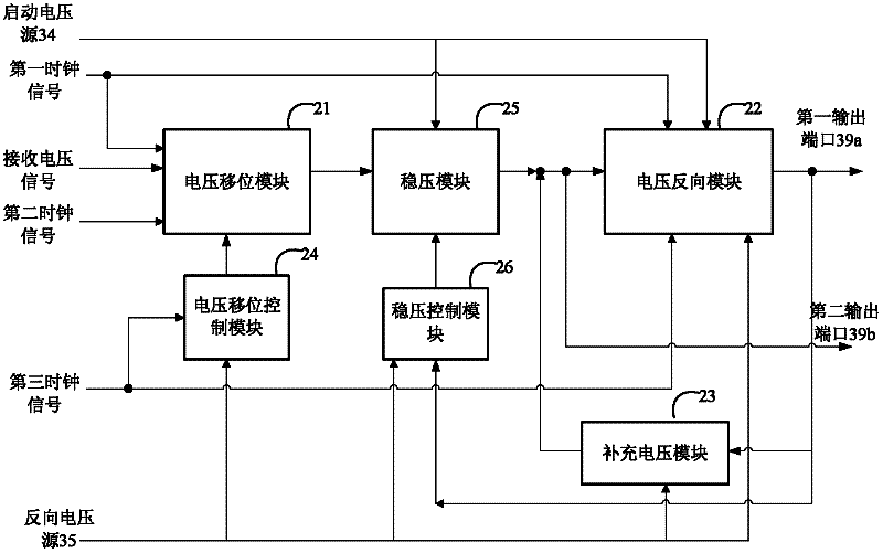
[0051] Such as image 3 Shown is a schematic diagram of the specific circuit structure of the present invention.
[0052] In this embodiment, the starting voltage signals are provided by CLK1, CLK2, and CLK3, and the starting voltage source 34 and the reverse voltage source 35 respectively provide a voltage in the same direction as the starting voltage and a voltage opposite to the starting voltage. Among them, CLK1, a voltage shift module startup voltage with a length of one-third cycle occurs every one-third cycle; CLK2, a voltage shift module start voltage with a length of one-third cycle occurs every one-third cycle voltage, and the startup voltage lags one-third of the cycle of the startup voltage of the first clock signal; CLK3, a voltage shift module startup voltage with a length of one-third of a cycle appears every one-third of the cycle, and the startup voltage lags behind The start-up voltage of the second clock signal CLK2 is one-third of the cycle.
[0053] The ...
Embodiment 3
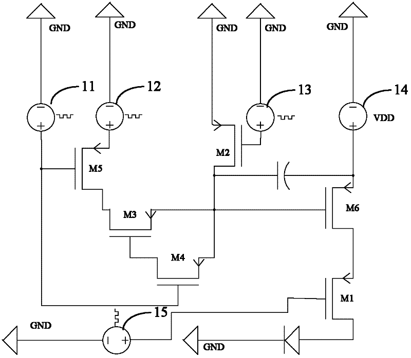
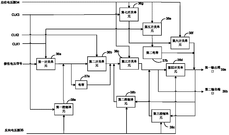
[0100] The switch unit and the control unit in the present invention may be any one or a combination of field effect transistors, triodes and thin film transistors. In this embodiment, N-channel thin film transistors are used as the components of the switch unit and the control unit, and the circuit structure is as follows image 3 and Figure 4 shown.
[0101] In this embodiment, three clock signals, a high-voltage power supply and a low-voltage power supply, control the on and off of elements in the shift register. Since this embodiment uses an N-channel thin film transistor, the starting voltage source of this embodiment is a high voltage, and the reverse voltage source is a low voltage. In this embodiment, the three clock signals include: CLK1, a voltage shift module startup voltage with a length of one third of a cycle appears every third cycle; CLK2, a length of three minutes appears every third cycle One-period voltage shift module startup voltage, and the startup vo...
Embodiment 4
[0126] The switch unit and the control unit in the present invention may be any one or a combination of field effect transistors, triodes and thin film transistors. In this embodiment, P-channel thin film transistors are used as the components of the switch unit and the control unit, and the circuit structure is as follows image 3 and Figure 6 shown.
[0127] In this embodiment, three clock signals, a high-voltage power supply and a low-voltage power supply, control the on and off of elements in the shift register. Since this embodiment uses a P-channel thin film transistor, the starting voltage source of this embodiment is a low voltage, and the reverse voltage source is a high voltage. Wherein, in this embodiment, the three clock signals include: CLK1, a voltage shift module startup voltage with a length of one third of a cycle appears every third cycle; CLK2, a length of 1 / 3 cycle appears every one third of the cycle. The start-up voltage of the voltage shift module of...
PUM
 Abstract
Description
Claims
Application Information
 - R&D Engineer
- R&D Manager
- IP Professional
- Industry Leading Data Capabilities
- Powerful AI technology
- Patent DNA Extraction
Browse by: Latest US Patents, China's latest patents, Technical Efficacy Thesaurus, Application Domain, Technology Topic.
© 2024 PatSnap. All rights reserved.Legal|Privacy policy|Modern Slavery Act Transparency Statement|Sitemap