Pulse output circuit, shift register, and display device

a shift register and output circuit technology, applied in pulse technique, pulse details, instruments, etc., can solve the problems of difficult to effectively reduce the manufacturing cost of such display devices, source region and drain region cannot be separated from each other, etc., to achieve the effect of reducing the number of manufacturing steps and low cos

Inactive Publication Date: 2005-08-09
SEMICON ENERGY LAB CO LTD
View PDF54 Cites 137 Cited by
  • Summary
  • Abstract
  • Description
  • Claims
  • Application Information

AI Technical Summary

Benefits of technology

[0021]In view of the above-described problem, an object of the present invention is to provide a pulse output circuit which is formed by using only TFTs of one polarity, which can therefore be fabricated at a low cost by performing a reduced number of manufacturing steps, and from which an output can be obtained without being attenuated in amplitude, and a shift register using the output circuit.

Problems solved by technology

However, the source region and the drain region cannot be discriminated from each other because of a structural characteristic of the TFT.
However, it is difficult to effectively reduce the manufacturing cost of such display devices by improving the yield, etc.
However, there is a problem described below with each of the inverter using a TFT as a load and the inverter using a resistor as a load. FIG. 9D shows the waveform of the output from the inverter using the TFT 903 as a load.

Method used


Image

  • Pulse output circuit, shift register, and display device
  • Pulse output circuit, shift register, and display device
  • Pulse output circuit, shift register, and display device

Examples


embodiment 1

(Embodiment 1)

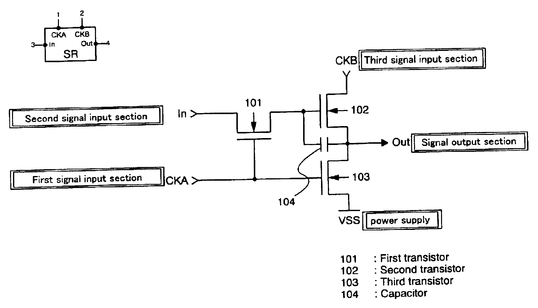
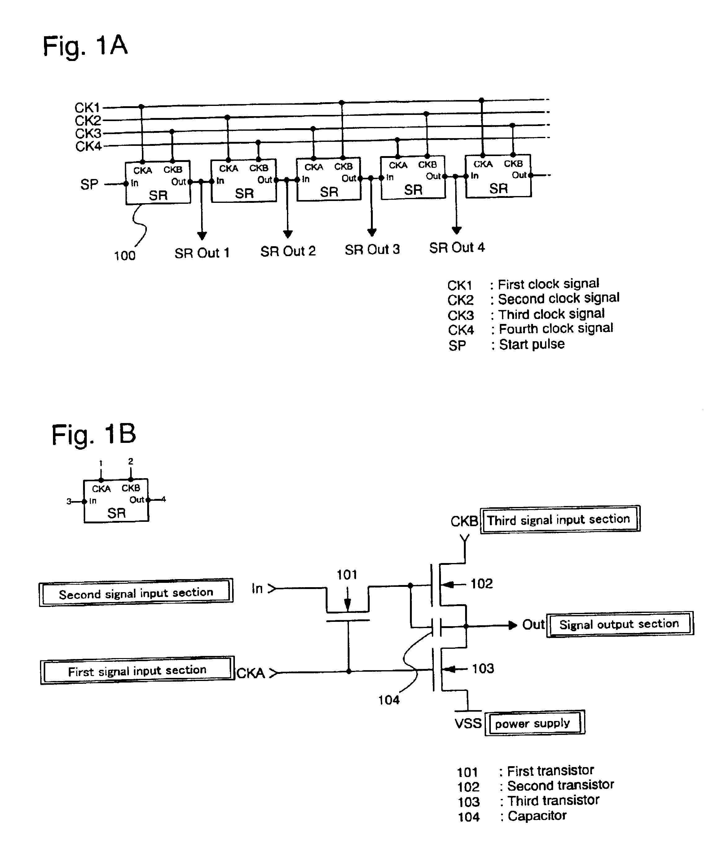
[0143]FIG. 3A shows an example of a shift register arranged in such a manner that a scanning direction inverting function is added to the shift register described above in the description of the embodiment mode of the present invention. The shift register of this embodiment uses additional input signals: an input change signal (LR) and an inverted input change signal (RL) other than those used in the circuit shown in FIG. 1A.

[0144]FIG. 3B shows details of the configuration of the pulse output circuit corresponding to one stage represented by a block 300 in FIG. 3A. The portion of the pulse output circuit constituted by TFTs 301 to 303 and a capacitor 304 is the same as the circuit shown in FIG. 1B, and the pulse output circuit of this embodiment has an input change circuit 310 constituted by a switch formed of TFTs 305 and 306, a fifth signal input section, and a sixth signal input section.

[0145]Each of output electrodes of TFTs 305 and 306 is connected to an input ele...

embodiment 2

(Embodiment 2)

[0149]An example of a display device fabricated by using only TFTs of one polarity will be described.

[0150]FIG. 12 is a diagram schematically showing the entire display device. A source signal line driver circuit 1201, a gate signal line driver circuit 1202, and a pixel portion 1203 are formed integrally with each other on a substrate 1200. A section of the pixel portion 1203 shown in a frame 1210 indicated by the dotted line is a segment for forming one pixel. The example of the pixel shown in FIG. 12 is a pixel of a liquid crystal display device. ON / OFF control of each pixel is performed by using one TFT in the pixel (hereinafter referred to as “pixel TFT”) when charge is applied to one electrode of the liquid crystal device. Signals (clock signals, a start pulse, etc.) for driving the source signal line driver circuit 1201 and the gate signal line driver circuit 1202 are externally supplied via a flexible printed circuit (FPC) 1204.

[0151]The substrate having the pix...

embodiment 3

(Embodiment 3)

[0174]In the embodiment mode of the present invention and the above embodiments of the present invention, examples of the circuits formed by using only n-channel TFTs have been shown. However, similar circuits may be formed by using only p-channel TFTs and by interchanging the power supply potential levels.

[0175]FIGS. 13A and 13B illustrate an example of a shift register formed by using only p-channel TFTs. The structure shown in the block diagram of FIG. 13A is the same as that of the shift register shown in FIGS. 1A and 1B, which is formed by using only n-channel TFTs. A block 1300 in FIG. 13A represents a pulse output circuit forming one stage for outputting a sampling pulse. The shift register shown in FIG. 13A differs from the shift register formed by using only n-channel TFTs in that the levels of the power supply potentials are reversed as shown in FIG. 13B.

[0176]FIG. 14 shows a timing chart and output pulses. The operation of each section is the same as that in...


PUM


Abstract

A circuit is provided which is constituted by TFTs of one conductivity type, and which is capable of outputting signals of a normal amplitude. When an input clock signal CK1 becomes a high level, each of TFTs (101, 103) is turned on to settle at a low level the potential at a signal output section (Out). A pulse is then input to a signal input section (In) and becomes high level. The gate potential of TFT (102) is increased to (VDD−V thN) and the gate is floated. TFT (102) is thus turned on. Then CK1 becomes low level and each of TFTs (101, 103) is turned off. Simultaneously, CK3 becomes high level and the potential at the signal output section is increased. Simultaneously, the potential at the gate of TFT (102) is increased to a level equal to or higher than (VDD+V thN) by the function of capacitor (104), so that the high level appearing at the signal output section (Out) becomes equal to VDD. When SP becomes low level; CK3 becomes low level; and CK1 becomes high level, the potential at the signal output section (Out) becomes low level again.

Description

BACKGROUND OF THE INVENTION[0001]1. Field of the Invention[0002]The present invention relates to a pulse output circuit, a shift register and a display device. Note that in this specification, display devices include a liquid crystal display device using a liquid crystal display element as a pixel, and a self-luminous display device using a self-luminous element, e.g., an electroluminecent (EL) element. Driver circuits for a display device are circuits which perform processing for displaying an image by inputting image signals to pixels arranged in the display device, and which include pulse output circuits, e.g., a shift register and an inverter, and amplifier circuits.[0003]2. Description of the Related Art[0004]In recent years, display devices having a semiconductor thin film formed on an insulating substrate such as a glass substrate, particularly active matrix display devices using thin film transistors (TFTs) have become widely available and have been used in various products....

Claims


Application Information

Patent Timeline
Patent Type & Authority Patents(United States)
IPC IPC(8): G09G3/36G11C19/28G11C19/00H03K19/096H03K19/017H03K19/01
CPCG09G3/3648G09G3/3688G11C19/00G11C19/28H03K19/01735H03K19/096G09G2300/0408G09G2310/0283G09G2310/0297H01L2924/0002H01L2924/00G09G3/36G09G3/3614G09G2300/0426G09G2310/0254G09G2310/0286G09G2310/0289G09G2310/0291G09G2310/08
Inventor NAGAO, SHOUAZAMI, MUNEHIROTANADA, YOSHIFUMI
Owner SEMICON ENERGY LAB CO LTD
Why Eureka
Try Eureka