

Shift register, semiconductor device, display device, and electronic device
a shift register and semiconductor technology, applied in static indicating devices, instruments, electroluminescent light sources, etc., can solve the problems of shift register circuit malfunction and transistor formed of amorphous semiconductors deteriorating in characteristics, so as to suppress the deterioration of transistor characteristics and reduce noise
- Summary
- Abstract
- Description
- Claims
- Application Information
AI Technical Summary
Benefits of technology
Problems solved by technology
Method used
Image

Examples
embodiment mode 1
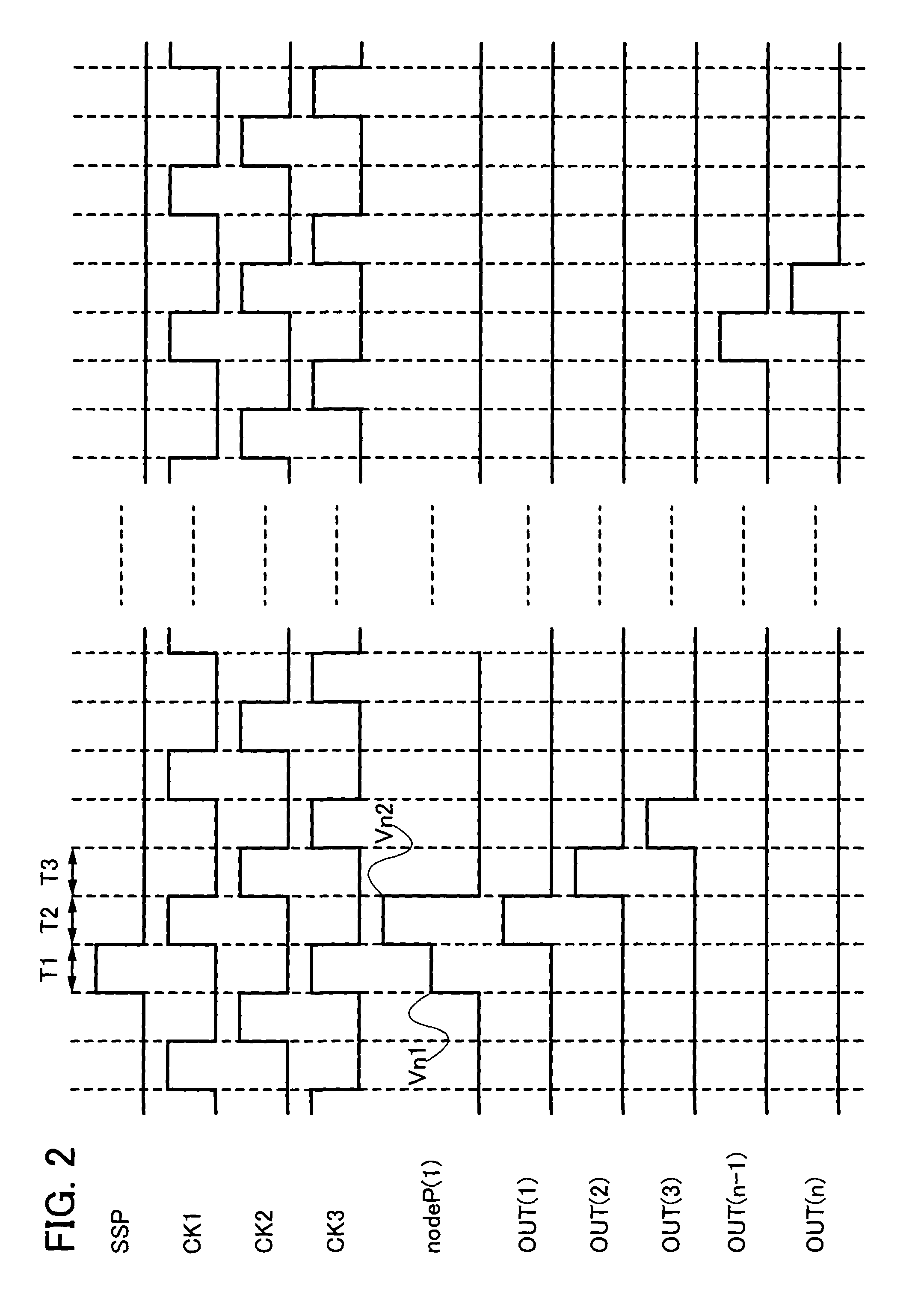
[0114]In this embodiment mode, description is made with reference to FIGS. 1 to 4 of a configuration and an operation of a shift register circuit in which a noise is reduced by outputting VSS at regular intervals for reducing a noise of an output voltage in a non-selection period.
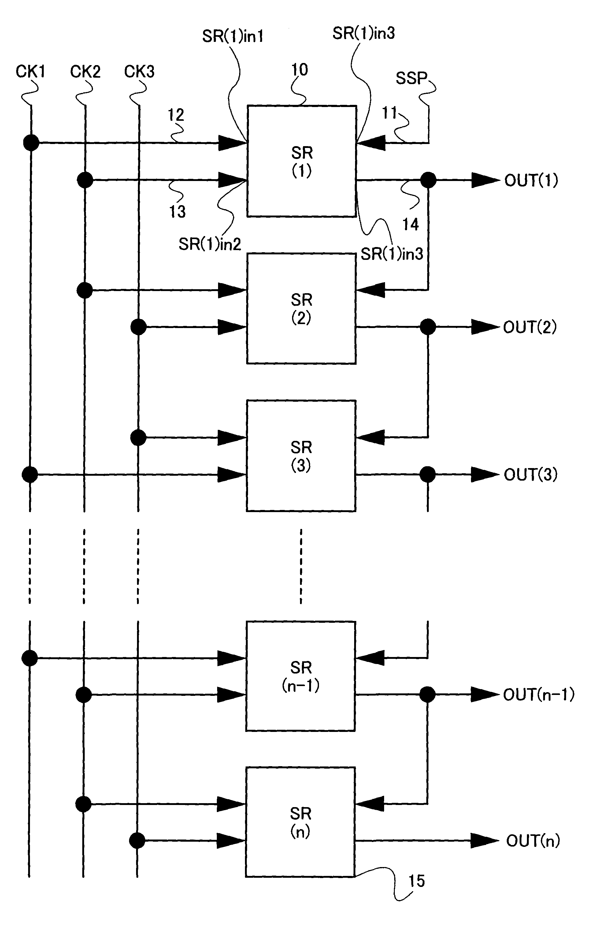
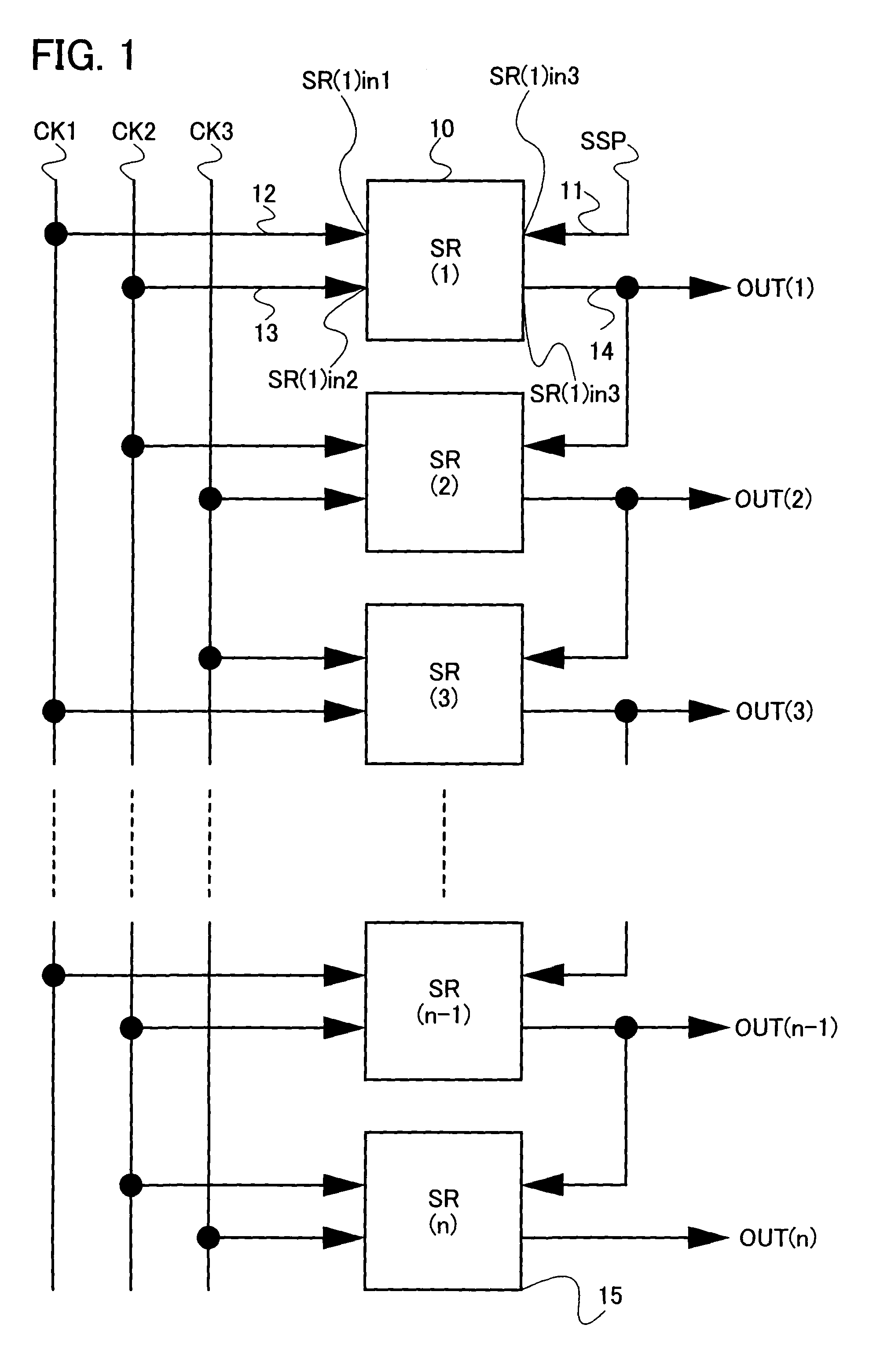
[0115]As shown in FIG. 1, a circuit 10 constitutes a shift register circuit with n (n is a natural number of 2 or larger) circuits SR(1) to SR(n) connected in series.
[0116]An input terminal 11 is an input terminal for inputting a start pulse in SR(1) as the circuit 10 of a first stage and for inputting an output from an output terminal 14 of a preceding stage in the circuits 10 of second to n-th stages. An input terminal 12 is an input terminal for sequentially inputting CK1, CK2, and CK3 in such a manner that CK1 is inputted as a clock signal to SR(1) as the circuit 10 of the first stage, CK2 is inputted as a clock signal to SR(2) as the circuit 10 of the second stage, CK3 is inputted as a clock signal to ...
embodiment mode 2
[0164]In this embodiment mode, description is made with reference to FIGS. 2 and 5 to 7 of a configuration and an operation of a shift register circuit in which a noise in an output voltage in a non-selection period is reduced by outputting VSS at regular intervals.
[0165]As shown in FIG. 5, a circuit 50 forms a shift register circuit by n (n is a natural number of two or larger) circuits SR(1) to SR(n) connected in series.
[0166]An input terminal 51 is an input terminal for inputting a start pulse in SR(1) as the circuit 50 of a first stage and for inputting an output from an output terminal 55 of a preceding stage in SR(2) as the circuits 50 of second to n-th stages. An input terminal 52 is an input terminal for sequentially inputting CK1, CK2, and CK3 in such a manner that CK1 is inputted as a clock signal to SR(1) as the circuit 50 of the first stage, CK2 is inputted as a clock signal to SR(2) as the circuit 50 of the second stage, CK3 is inputted as a clock signal to SR(3) as the...
embodiment mode 3
[0212]In this embodiment mode, description is made with reference to FIGS. 2, 5, and 8 to 10 of a configuration and an operation of a shift register circuit in which a noise in an output voltage in a non-selection period is reduced by outputting VSS in the non-selection period.
[0213]The configuration of the shift register circuit shown in FIG. 5 and an operation thereof can be similar to those described in Embodiment Mode 2.
[0214]Description is made of a configuration of SR(1) as the circuit 50 of a first stage with reference to FIG. 8. The circuit 50 shown in FIG. 8 is configured with the input terminal 51, the input terminal 52, the input terminal 53, the input terminal 54, the output terminal 55, the transistor 31, the transistor 32, the capacitor 33, a circuit 81, a circuit 82, and a circuit 83.
[0215]The input terminal 51, the input terminal 52, the input terminal 53, the input terminal 54, the output terminal 55, the transistor 31, the transistor 32, and the capacitor 33 are si...
PUM
 Abstract
Description
Claims
Application Information