Configuration shift register

a technology of configuration shift and register, applied in the direction of computation using denominational number representation, pulse technique, instruments, etc., can solve the problems of creating time inefficiencies and increasing the burden of repeated reprogramming

Inactive Publication Date: 2006-09-26
ALTERA CORP
View PDF22 Cites 129 Cited by
  • Summary
  • Abstract
  • Description
  • Claims
  • Application Information

AI Technical Summary

Benefits of technology

[0015]The present invention provides an electronic device having configuration elements connected as a shift register, the configuration elements being relevant to a particular programmable function or subset of programmable functions such as I / O. The configuration shift register may be loaded with new data without having to reprogram other configuration elements of the electronic device. In an exemplary embodiment, the electronic device is a programmable logic device (PLD). In an aspect of an exemplary embodiment, shadow register elements allow programming data from one configuration to be maintained for-particular IOs while new programming data for another configuration is loaded into the configuration shift register. In an aspect of a particular embodiment, a JTAG port of the PLD is used to load data into the configuration shift register and a demultiplexer selectively directs data to either a boundary scan chain of elements used for JTAG test data or to the configuration shift register. In another aspect of a particular embodiment, selected configuration elements in the configuration shift register are connected to pins for parallel loading of configuration data as an alternative to sequential loading of data into the configuration shift register from a single pin. In an alternative embodiment, cells of configuration elements forming the configuration shift register are interleaved with cells of elements used for JTAG test data forming a single shift register that may be used for rapidly reconfiguring particular programmable functions of the electronic device and also may be for boundary scan test purposes.

Problems solved by technology

However, providing a PLD that has a large grid of configuration elements, for example, as large as 2,000×2,000 configuration elements organized in rows and columns, can create time inefficiencies during testing when particular subsets functions of the PLD may need to be repeatedly reprogrammed.
However, when testing the PLD, it may be necessary to frequently retest the PLD with different configurations.
As the number of configuration elements in a PLD grows, this repeated reprogramming can become increasingly burdensome, particularly when testing multiple PLDs, and particularly given the increasing need to test a PLD with several different configurations of its I / O elements.

Method used


Image

  • Configuration shift register
  • Configuration shift register
  • Configuration shift register

Examples


Embodiment Construction

[0022]The following description is presented to enable any person skilled in the art to make and use the invention, and is provided in the context of particular applications and their requirements. Various modifications to the exemplary embodiments will be readily apparent to those skilled in the art, and the generic principles defined herein may be applied to other embodiments and applications without departing from the spirit and scope of the invention. Thus, the present invention is not intended to be limited to the embodiments shown, but is to be accorded the widest scope consistent with the principles and features disclosed herein.

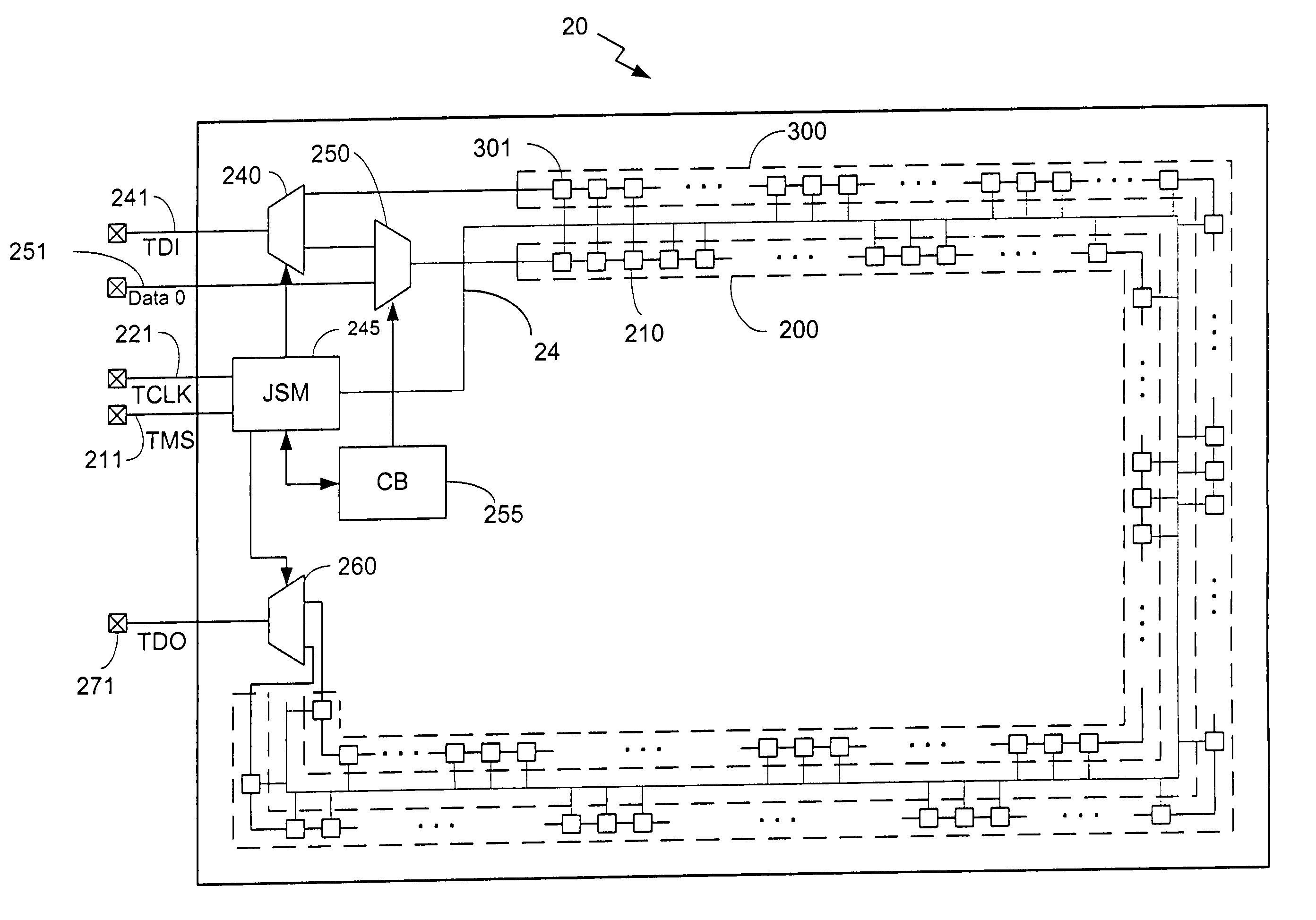
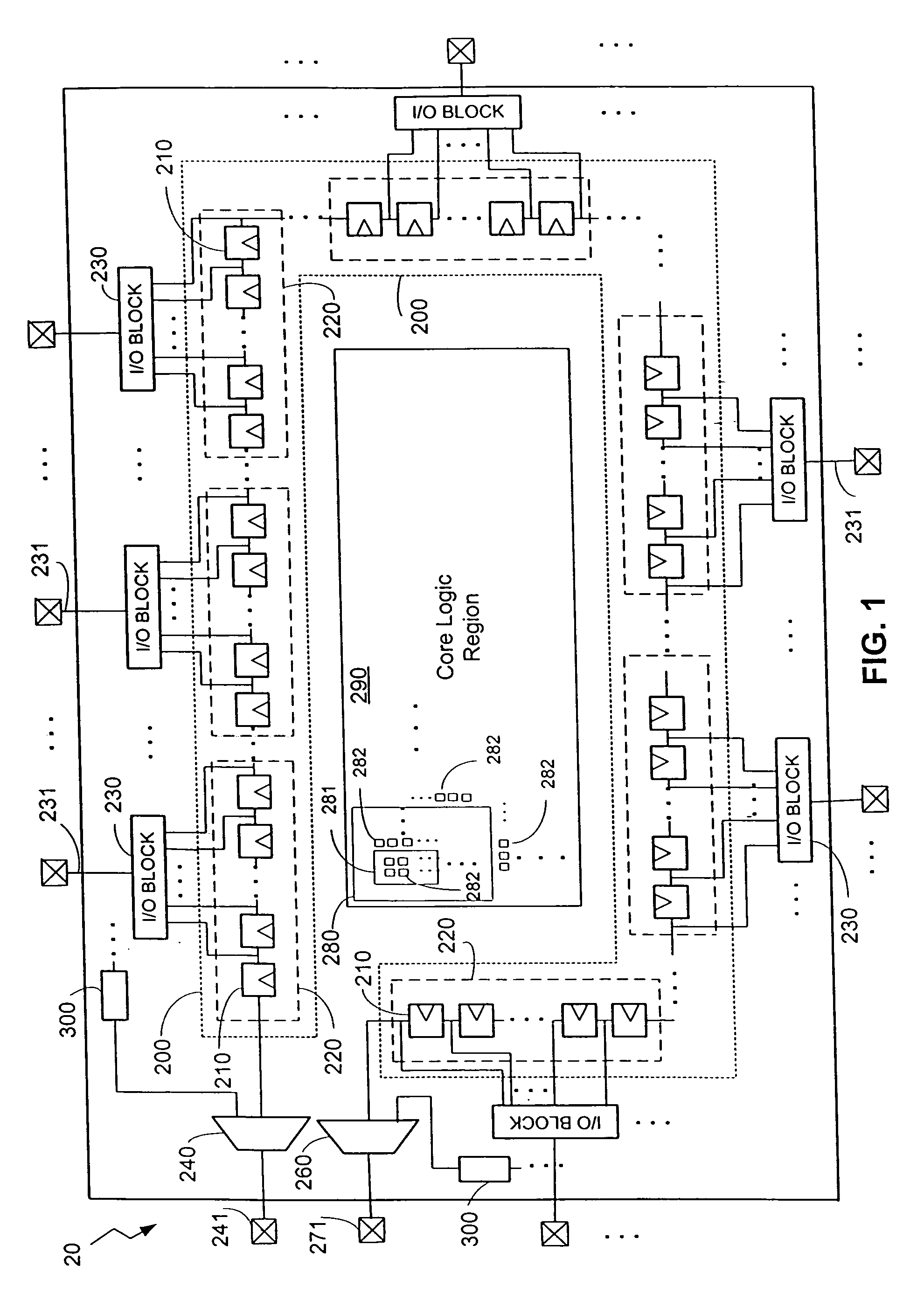
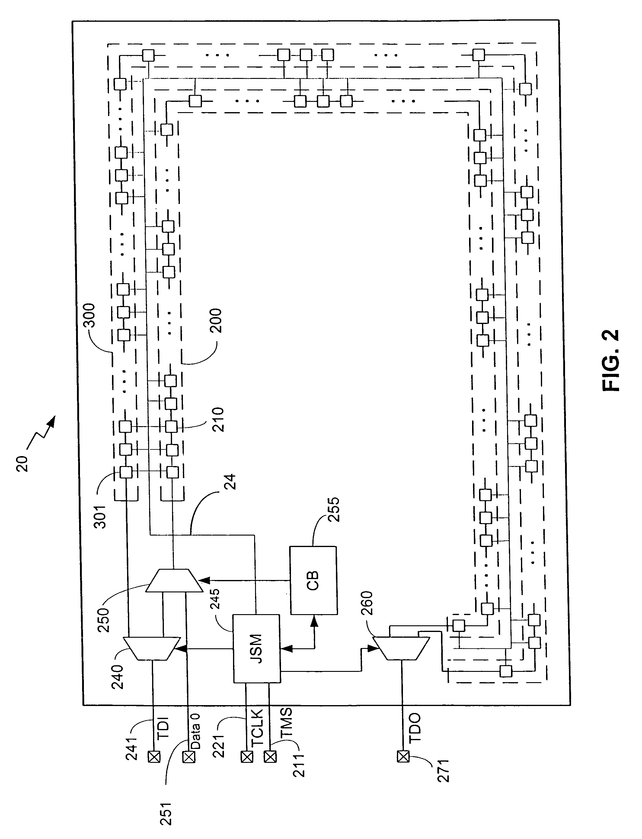
[0023]Referring to FIG. 1, a PLD 20 includes a core logic region 290 and an configuration shift register 200 outside of region 290. Configuration shift register 200 is coupled to a plurality of I / O blocks 230. Core logic region 290 includes logic elements (LEs) 281 grouped in blocks forming LABs 280. Only one LAB 280 and LE 281 is shown in any detail;...


PUM


Abstract

An electronic device comprises a first plurality of configuration elements connected as a shift register for programming a subset of the programmable functions of the electronic device. The subset of programmable functions may be reprogrammed by loading configuration data into the first plurality of configuration elements such that the subset of programmable functions may be reprogrammed without necessarily reprogramming other programmable functions of the electronic device.

Description

CROSS-REFERENCE TO RELATED APPLICATIONS[0001]This application is a continuation of U.S. patent application Ser. No. 10 / 278,177, filed on Oct. 21, 2002, issued as U.S. Pat. No. 6,842,039.BACKGROUND OF THE INVENTION[0002]1. Field of the Invention[0003]The present invention relates to a configuration shift register for use in configuring programmable logic devices or other similar devices.[0004]2. Description of Related Art[0005]Programmable logic devices (“PLDs”) (also sometimes referred to as CPLDs, PALs, PLAs, FPLAs, EPLDs, EEPLDs, LCAs, FPGAs, or by other names), are well-known integrated circuits that provide the advantages of fixed integrated circuits with the flexibility of custom integrated circuits. Such devices are well known in the art and typically provide an “off the shelf” device having at least a portion that can be electrically programmed to meet a user's specific needs. Application specific integrated circuits (“ASICs”) have traditionally been fixed integrated circuits...

Claims


Application Information

Patent Timeline
Patent Type & Authority Patents(United States)
IPC IPC(8): H03K19/173H03K19/177
CPCH03K19/1774H03K19/17756H03K19/17752H03K19/17744
Inventor GUZMAN, MARIOLANE, CHRISLEE, ANDY L.NGO, NINH
Owner ALTERA CORP
Why Eureka
Try Eureka