Check patentability & draft patents in minutes with Patsnap Eureka AI!

TFT (thin film transistor) array substrate, manufacturing method of TFT array substrate and display device

An array substrate and substrate technology, applied in the field of electronic device display, can solve the problems of reducing the aperture ratio of pixel units, affecting the contrast ratio of electronic display devices, etc., and achieve the effect of increasing the aperture ratio

Active Publication Date: 2012-09-05
BOE TECH GRP CO LTD
View PDF5 Cites 3 Cited by
  • Summary
  • Abstract
  • Description
  • Claims
  • Application Information

AI Technical Summary

Problems solved by technology

In order to reduce the coupling capacitance between the pixel electrode and the source electrode, the overlapping area between the pixel electrode and the source electrode is generally reduced by reducing the area of ​​the pixel electrode, so that the coupling capacitance between the source electrode and the pixel electrode is reduced. , but this also reduces the aperture ratio of the pixel unit, thereby affecting the contrast of the electronic display device driven by the TFT array substrate

Method used


Image

  • TFT (thin film transistor) array substrate, manufacturing method of TFT array substrate and display device
  • TFT (thin film transistor) array substrate, manufacturing method of TFT array substrate and display device
  • TFT (thin film transistor) array substrate, manufacturing method of TFT array substrate and display device

Examples


Embodiment Construction

[0014] The technical solutions in the embodiments of the present invention will be clearly and completely described below with reference to the accompanying drawings in the embodiments of the present invention. Obviously, the described embodiments are only a part of the embodiments of the present invention, but not all of the embodiments. Based on the embodiments of the present invention, all other embodiments obtained by those of ordinary skill in the art without creative efforts shall fall within the protection scope of the present invention.

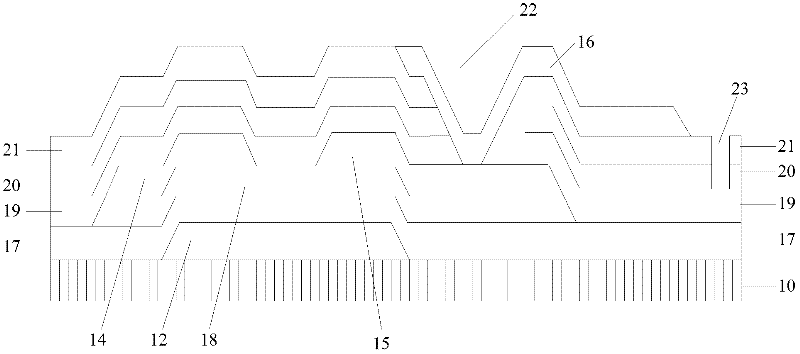
[0015] An embodiment of the present invention provides a TFT array substrate, such as figure 1 shown, figure 1 is a cross-sectional view of the TFT array substrate along the direction of the TFT region parallel to the gate line, wherein figure 1 The data lines and gate lines are not shown. The TN-type TFT array substrate is taken as an example for specific description below, including: a substrate 10, a gate line and a gate 12 forme...


PUM


Abstract

The embodiment of the invention provides a TFT (thin film transistor) array substrate, a manufacturing method of the TFT array substrate and a display device. According to the embodiment of the invention, the coupling capacitance of the TFT array substrate can be reduced, the opening rate of a pixel unit can be improved and the contrast of electronic display equipment can be enhanced. The TFT array substrate comprises a substrate, and a grid line, a grid electrode, a grid insulating layer, a semiconductor active layer, a data wire, a source electrode, a drain electrode and a pixel electrode, which are formed on the substrate, wherein the data wire is connected with the source electrode, the drain electrode is connected with the pixel electrode, a first insulating layer, a metal layer and a second insulating layer are sequentially formed among the source electrode, the drain electrode and the pixel electrode, and the metal layer is connected with a voltage stabilization signal wire through a metal layer lead through hole. The TFT array substrate is applied to electronic display equipment actively driven by the TFT array substrate.

Description

technical field [0001] The invention relates to the display field of electronic equipment, in particular to a TFT array substrate, a manufacturing method of the TFT array substrate and a display device. Background technique [0002] With the development of information and network, electronic display technology has been widely used as a technology. Currently, LCD (Liquid Crystal Display) display devices are widely used, and electronic paper, which is a substitute for people to read paper, is also developing rapidly. [0003] The active driving method of LCD display devices and electronic paper display devices usually adopts active matrix driving technology, such as TFT (Thin Film Transistor) array substrate driving method. [0004] In the process of realizing the TFT array substrate, coupling capacitance is usually generated between the pixel electrode and the source electrode. In order to reduce the coupling capacitance between the pixel electrode and the source electrode,...

Claims


Application Information

Patent Timeline
Patent Type & Authority Applications(China)
IPC IPC(8): G02F1/1362G02F1/1368H01L27/12H01L21/77
CPCH01L27/124H01L27/1259H01L29/41733H01L29/4908
Inventor 盖翠丽张卓
Owner BOE TECH GRP CO LTD
Features
  • R&D
  • Intellectual Property
  • Life Sciences
  • Materials
  • Tech Scout
  • Unparalleled Data Quality
  • Higher Quality Content
  • 60% Fewer Hallucinations
Learn More