Printed circuit board
A printed circuit board and transmission line electrical technology, applied in the direction of printed circuit components, etc., can solve problems affecting signal transmission quality, differential signal impedance discontinuity, etc., and achieve the effect of ensuring transmission quality
- Summary
- Abstract
- Description
- Claims
- Application Information
AI Technical Summary
Problems solved by technology
Method used
Image

Examples
Embodiment Construction
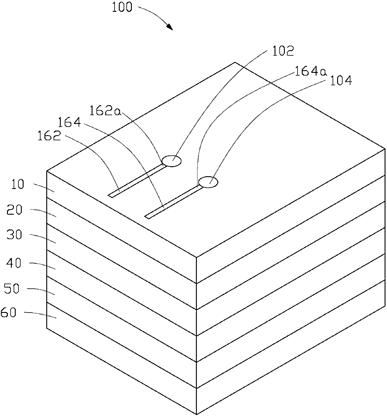
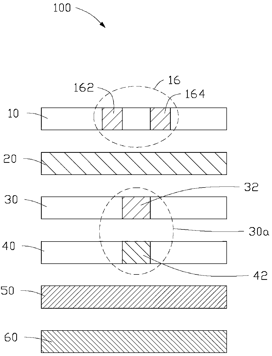
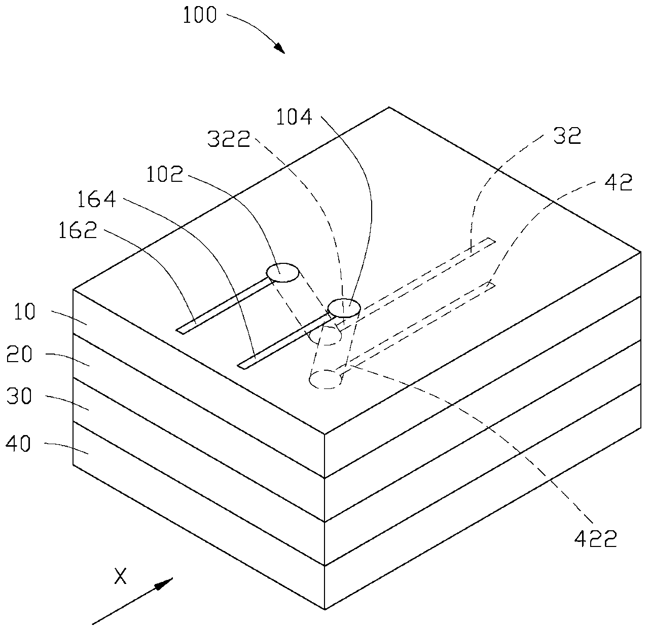
[0014] see figure 1 and figure 2 , is the printed circuit board 100 according to the first embodiment of the present invention. The printed circuit board 100 includes a first signal layer 10, a first reference layer 20, a second signal layer 30, a third signal layer 40, a second reference layer 50 and a bottom layer stacked in sequence from top to bottom. 60.
[0015] Please combine image 3 and Figure 4 , the first signal layer 10 includes a wiring layer 12 and a connection layer 14 opposite to the wiring layer 12 . A first differential pair 16 is arranged on the wiring layer 12 in an edge-coupling manner. The first differential pair 16 includes a first differential transmission line 162 and a second differential transmission line 164 . The first differential transmission line 162 is adjacent to and coupled to the second differential transmission line 164 in parallel. The first differential transmission line 162 includes a first connection end 162a. The second diffe...
PUM
 Abstract
Description
Claims
Application Information
PatSnap Eureka turns technology decisions into work you can execute. Powered by our Innovation Knowledge Graph, it runs expert workflows across engineering, life sciences, materials and intellectual property. Get your review-ready output in minutes.


