Input device
An input device and resistance layer technology, applied in the input/output process of data processing, instruments, electrical digital data processing, etc., can solve the problem of no record of the wiring layer structure, and achieve linear, excellent operational responsiveness, and simple structure. , low cost effect
- Summary
- Abstract
- Description
- Claims
- Application Information
AI Technical Summary
Problems solved by technology
Method used
Image

Examples
Embodiment Construction
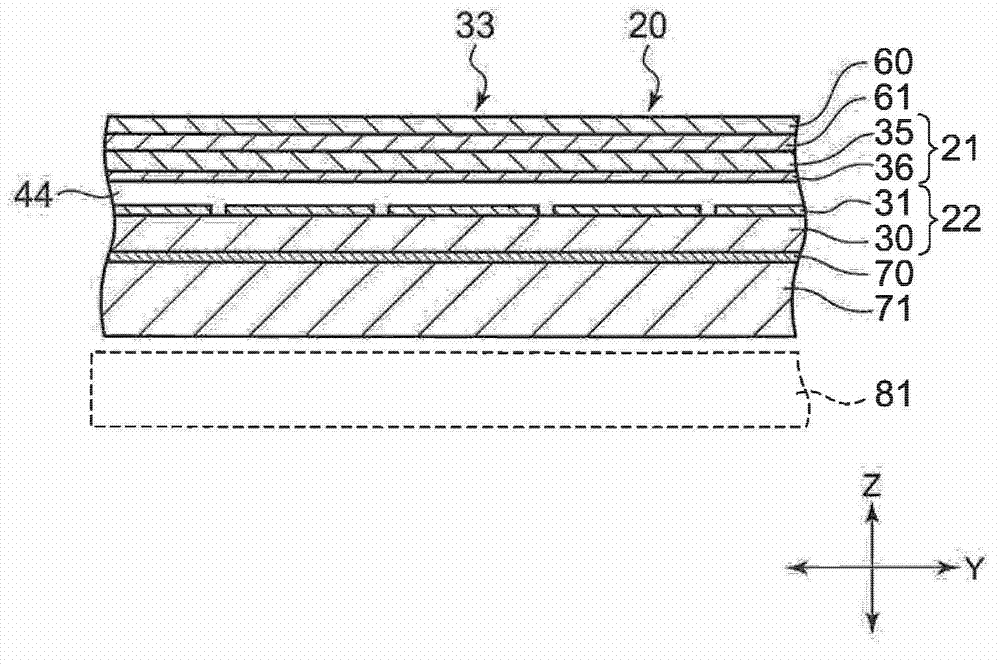
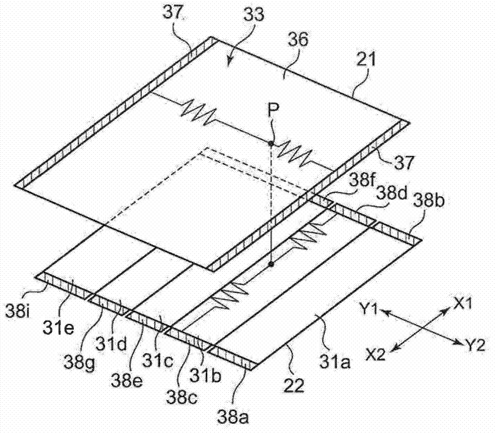
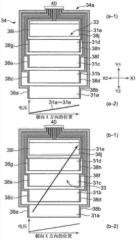
[0035] figure 1 It is a partial longitudinal cross-sectional view (along image 3 Partial vertical cross-sectional view cut in the height direction in the Y1-Y2 direction), figure 2 is an explanatory diagram showing the detection operation of the input device, image 3 (a-1) is a plan view (schematic diagram) of the first divided resistance layer and the wiring layer provided on the first substrate constituting the input device of the present embodiment, image 3 (a-2) is a graph (schematic diagram) showing the relationship between the position toward the lateral direction (X) and the voltage gradient of the voltage applied to each first divided wiring layer, image 3 (b-1) means that along the direction of the arrow image 3 (a-1) is a plan view of the surface of the first split resistance layer being manipulated, image 3 (b-2) means along image 3 A graph (schematic diagram) of the relationship between the operating position in the lateral direction (X) and the volta...
PUM
 Abstract
Description
Claims
Application Information
 - R&D Engineer
- R&D Manager
- IP Professional
- Industry Leading Data Capabilities
- Powerful AI technology
- Patent DNA Extraction
Browse by: Latest US Patents, China's latest patents, Technical Efficacy Thesaurus, Application Domain, Technology Topic.
© 2024 PatSnap. All rights reserved.Legal|Privacy policy|Modern Slavery Act Transparency Statement|Sitemap