Eureka AIR delivers breakthrough ideas for toughest innovation challenges, trusted by R&D personnel around the world.

Lithography system

A photosensitive element and optical fiber array technology, which can solve problems such as non-optimal aberrations when applied near or in the range of the projection space

Active Publication Date: 2012-12-12
ASML NETHERLANDS BV
View PDF5 Cites 0 Cited by
  • Summary
  • Abstract
  • Description
  • Claims
  • Application Information

AI Technical Summary

Problems solved by technology

[0009] Although the general configuration of the lithographic system described above has proven satisfactory, since it suffers from a non-optimal (at least less than expected) transmission of light and because it suffers from relatively large aberrations, it is noted that the disclosed tilt Defects in the lighting system

Method used


Image

  • Lithography system
  • Lithography system
  • Lithography system

Examples


Embodiment Construction

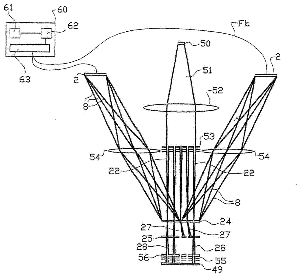
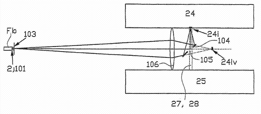
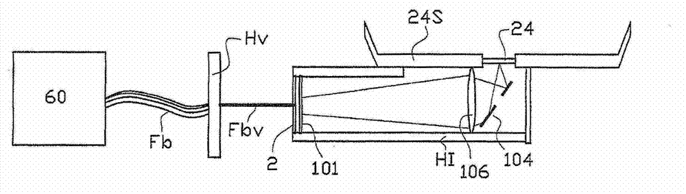
[0020] figure 1 shows a general side view of a prior art lithography system modified by the present invention, wherein at the modulation means end 2 of the light emitter or light carrier Fb, in particular the optical fiber Fb, using a lens An optical system, represented by 54, projects the light beam 8 onto the modulator array 24. The modulated light beam 8 from each optical fiber end is projected onto a photosensitive element, ie a photosensitive part of each modulator of said modulator array 24 . Specifically, each end of the fiber Fb is projected onto the modulator array. Each beam 8 has a portion of pattern data for controlling one or more modulators, the modulation of which forms a signaling system for delivering command of the modulator array based on the pattern data to achieve the desired image on said target surface .

[0021] figure 1 Also shown is a beam generator 50 which produces a diverging beam 51 of charged particles (in this example an electron beam). Usi...


PUM


Abstract

The inventions relates to a lithography system, particularly a charged particle and multiple-beam maskless lithography system which is used to project an image pattern to a target surface, wherein the image pattern is delivered to a exposure tool for projecting an image to a target surface. The system comprises a multiple-beam projection source and an optical device system, wherein multiple writing beams for writing patterns are generated, the writing beams are led to a blanking device array which comprises a modulator, a static deflector which deflects the writing beams based on the received pattern information is included, the modulator comprises a photosensitive elements used to receive modulated light beams, and the photosensitive elements are accommodated within the range near the deflector; and the optical device system comprises a light transmission component used to transmit pattern information signals and an optical fiber array used to emit the modulated light beams to the photosensitive elements, the optical fiber array is fixed on the outer shell of a clamp for the blanking device array, the end part of the optical fiber array is mechanically fixed on the outer shell, and therefore the tail ends of the optical fibers and the photosensitive elements are fixed opposite to each other.

Description

[0001] This application is a divisional application with application number 200680039487.8 filed on September 14, 2006 and titled "Photolithography System and Projection Method". technical field [0002] The present invention relates to a lithographic system for projecting an image pattern (image pattern) onto a target surface such as a wafer, wherein control data is coupled to a control unit to control the exposure projection by optical signals, thereby using free space interaction Connect (free space interconnect, free space interconnect), in particular to a system in which such a control unit is contained in close proximity or within the confines of the projection space, and more particularly to a multi-beam maskless lithography system. The present invention generally still relates to charged particle and light projection based lithographic systems. Background technique [0003] Such systems are known, for example, from the international patent publication WO2004038509 f...

Claims


Application Information

Patent Timeline
Patent Type & Authority Applications(China)
IPC IPC(8): G03F7/20H01J37/317
CPCG03F7/2014G03F7/70191G03F7/70208G03F7/70258G03F7/70291G03F7/70383G03F7/70508G03F7/70841G03F7/70991
Inventor 马尔科·扬·哈科·威兰斯泰恩·威廉·卡雷尔·赫尔曼·斯腾布林克吉多·德布尔雷姆科·亚赫奥谢·阿里安内·安妮特·卡斯特利杰恩
Owner ASML NETHERLANDS BV
Why Eureka
Eureka Blog
Learn More