PCB (Printed circuit board) butt welding method and PCB butt welding device

A technology of splicing and special-shaped boards, which is applied in the direction of assembling printed circuits with electrical components, can solve the problems of low utilization rate of boards, and achieve the effects of improving efficiency, reducing costs, and reducing production materials.

Active Publication Date: 2012-12-19
SHENZHEN PARTNER INFORMATION TECH
View PDF1 Cites 9 Cited by
  • Summary
  • Abstract
  • Description
  • Claims
  • Application Information

AI Technical Summary

Problems solved by technology

In the case that the Pcs that need to be assembled are special-shaped boards, but their pos

Method used


Image

  • PCB (Printed circuit board) butt welding method and PCB butt welding device
  • PCB (Printed circuit board) butt welding method and PCB butt welding device
  • PCB (Printed circuit board) butt welding method and PCB butt welding device

Examples


Embodiment Construction

[0071] In order to make the object, technical solution and advantages of the present invention clearer, the present invention will be further described in detail below in conjunction with the accompanying drawings and embodiments. It should be understood that the specific embodiments described here are only used to explain the present invention, not to limit the present invention.

[0072] Embodiments of the present invention relate to a panelizing method used in cutting PCB materials, and in particular to a panelizing method for special-shaped boards.

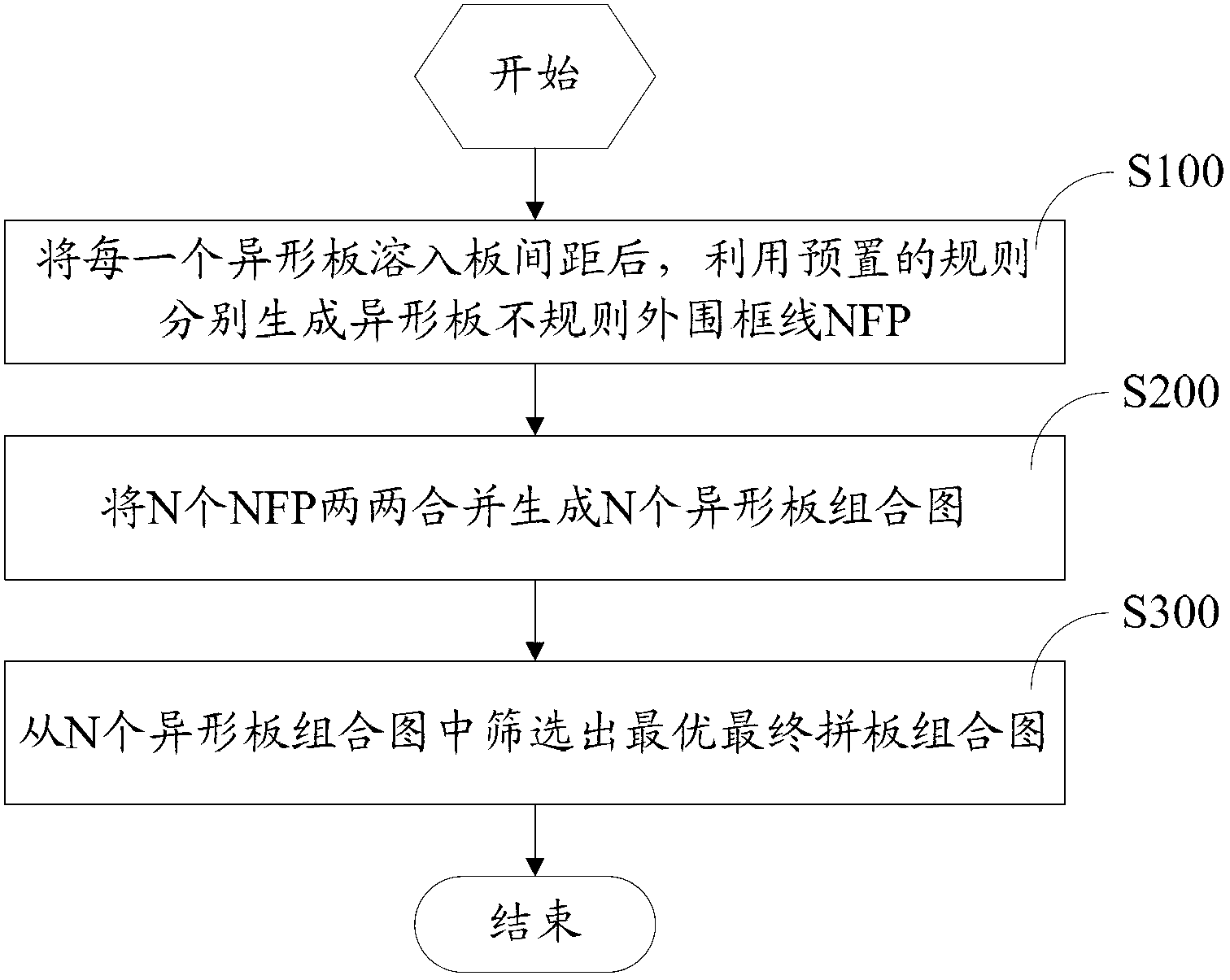
[0073] Please refer to figure 1 , is the PCB puzzle method proposed by the embodiment of the present invention, such as figure 1 As shown, the method includes the following steps:

[0074] S100: After dissolving each special-shaped board into the board spacing, use the preset rules to generate NFP (No Fit Polygon, irregular polygonal outline) of N special-shaped boards;

[0075] In the process of combining special-shaped pl...


PUM


Abstract

The invention relates to a PCB (Printed circuit board) butt welding method and a PCB butt welding device. The method comprises the following steps: integrating each irregular plate in the plate spacing, then generating irregular plate NFP (No Fit Polygon) by using a preset rule; combining every two NFP to generate N irregular plate combination charts; screening out the optimal butt welding combination chart from N irregular plate combination charts, wherein, N is an integral number which is larger than 1. According to the PCB butt welding method and the PCB butt welding device, the irregular plate integrated in the plate spacing is combined to generate the butt welding combination chart by using the preset rule, the optimal butt welding combination chart is screened out, the production efficiency of the PCB is improved, and production materials of the irregular plate is reduced, and the cost is reduced.

Description

technical field [0001] The invention relates to the technical field of PCB (Printed Circuit Board, printed circuit board), in particular to a method and a device for making up a PCB. Background technique [0002] At present, when it is necessary to combine multiple PCB products of the same process, it is usually used to manually combine multiple Pcs (the smallest shipment unit of a class of PCB products) into a Set (the smallest unit of production, which is determined by the Pcs synthesis). In the case that the Pcs that need to be assembled are special-shaped boards, but their positions in the Set are fixed, so that the utilization rate of the boards in the Set is usually low. Contents of the invention [0003] The main purpose of the present invention is to provide a method for splicing PCBs, aiming at reducing the cost of production materials for splicing PCB special-shaped boards. [0004] In order to achieve the above object, the present invention proposes a PCB pane...

Claims


Application Information

Patent Timeline
IPC IPC(8): H05K3/36
Inventor 曾宪雄符永高戴远征
Owner SHENZHEN PARTNER INFORMATION TECH
Why Eureka
Try Eureka