Bidirectional scanning control switch, grid drive circuit and working method
A technology for controlling switches and bidirectional scanning, which is applied in the field of gate drive circuits and bidirectional scanning switches. It can solve the problems of poor display flexibility, inability to meet display requirements, and single display mode. effect of demand
- Summary
- Abstract
- Description
- Claims
- Application Information
AI Technical Summary
Problems solved by technology
Method used
Image
Examples
Embodiment 1
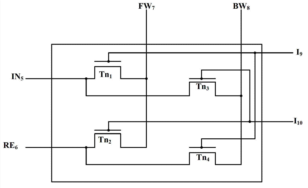
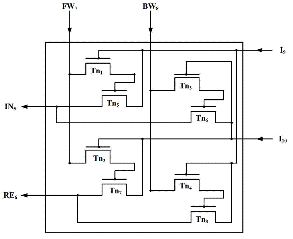
[0043] Such as figure 2 As shown, it is a schematic structural diagram of a bidirectional scanning control switch in Embodiment 1 of the present invention. The bidirectional scanning control switch includes: forward scanning control voltage port FW 7 , Reverse scan control voltage port BW 8 , the first input port I 9 , the second input port I 10 , the first output port IN 5 , the second output port RE 6 , the first transistor Tn 1 , the second transistor Tn 2 , the third transistor Tn 3 and the fourth transistor Tn 4 ,in:
[0044] first transistor Tn 1 The gate of the first input port I 9 connected, the first transistor Tn 1 The drain of the positive scan control voltage port FW 7 connected, the third transistor Tn 3 The gate of the second input port I 10 connected, the third transistor Tn 3 The drain of the reverse scan control voltage port BW 8 connected, the third transistor Tn 3 source of the first transistor Tn 1 The connection point where the source i...
Embodiment 2
[0056] Such as Figure 4 Shown is a flow chart of a working method of a bidirectional scanning control switch. In the second embodiment, a bidirectional scanning control switch with 4 transistors is taken as an example for illustration. The working method of the bidirectional scanning control switch is:
[0057] Step 101: Scan the control voltage port FW in the forward direction 7 Input high level, then execute step 102; In reverse scanning control voltage port BW 8 If a high level is input, step 105 is executed.
[0058] Step 102: At the first input port I 9 Input high level, then execute step 103; In the second input port 1 10 If a high level is input, step 104 is executed.
[0059] Step 103: first transistor Tn 1 is in the conduction state through the first transistor Tn with 1 The source is connected to the first output port IN 5 output high level.
[0060] Step 104: the second transistor Tn 2 is in the conduction state through the second transistor Tn with 2 T...
Embodiment 3
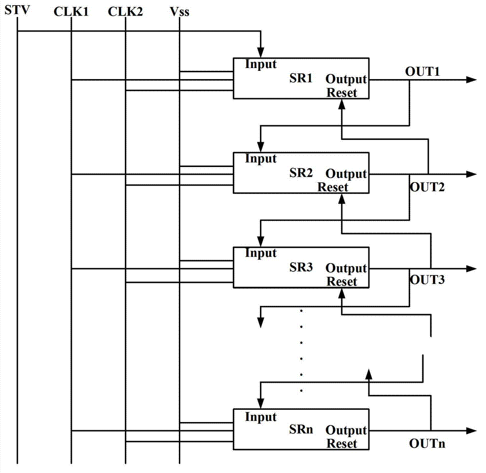
[0065] Such as Figure 5 Shown is a schematic structural diagram of a gate driving circuit in the third embodiment. The gate drive circuit also includes: a turn-on pulse STV supply line STV 13 , Forward scanning provides line L 14 , Reverse scanning provides line L 15 , n shift registers SR 1 ~SR n , n bidirectional scanning control switches CS 1 ~CS n , at least two switch units, the n is a positive integer, wherein:
[0066] Forward scan control voltage port FW in each bidirectional scan control switch 7 with a forward scan providing the line L 14 Connected, reverse scan control voltage port BW 8 with a reverse scan providing the line L 15 connected;
[0067] Turn on pulse STV supply line STV 13 Connected to the gate of a switching unit whose source is connected to the first bidirectional scan control switch CS 1 The first input port in I 9 Connected, the drain of the switching unit is connected to the forward scan supply line L 14 connected;
[0068] The mth...
PUM
 Abstract
Description
Claims
Application Information


