Pixel structure and manufacturing method of pixel structure

A pixel structure and manufacturing method technology, which is applied in semiconductor/solid-state device manufacturing, electrical components, transistors, etc., can solve the problems of reducing the display aperture ratio of the pixel structure and increasing the area of ​​the metal pattern, and achieve the effect of increasing the display aperture ratio

Active Publication Date: 2016-03-02
AU OPTRONICS CORP
View PDF3 Cites 0 Cited by
  • Summary
  • Abstract
  • Description
  • Claims
  • Application Information

AI Technical Summary

Problems solved by technology

However, such a design means that the area of ​​the metal pattern must be increased and the display aperture ratio of the pixel structure is reduced.

Method used


Image

  • Pixel structure and manufacturing method of pixel structure
  • Pixel structure and manufacturing method of pixel structure
  • Pixel structure and manufacturing method of pixel structure

Examples


Embodiment Construction

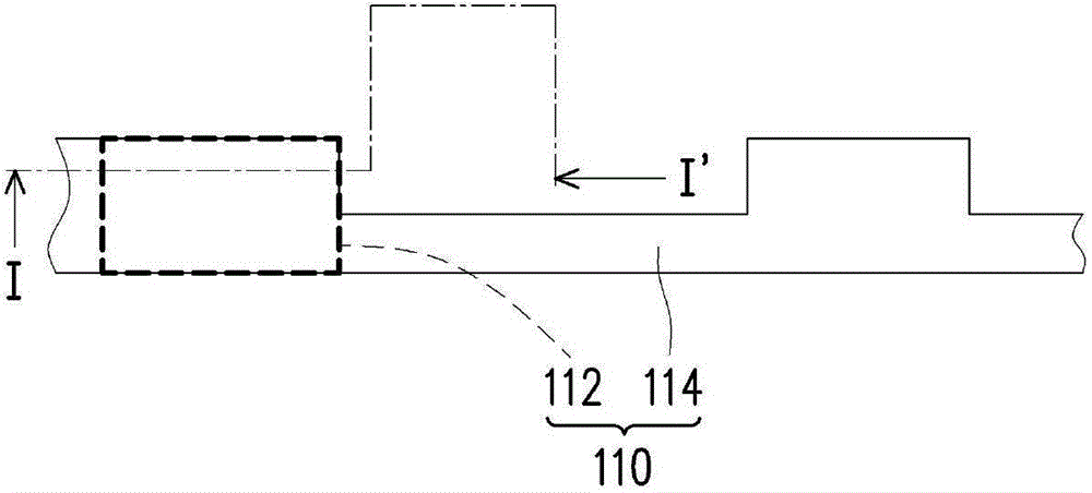
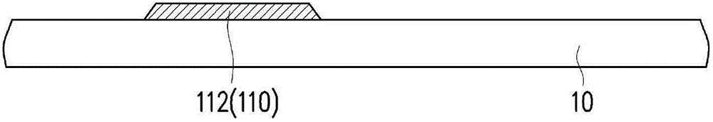
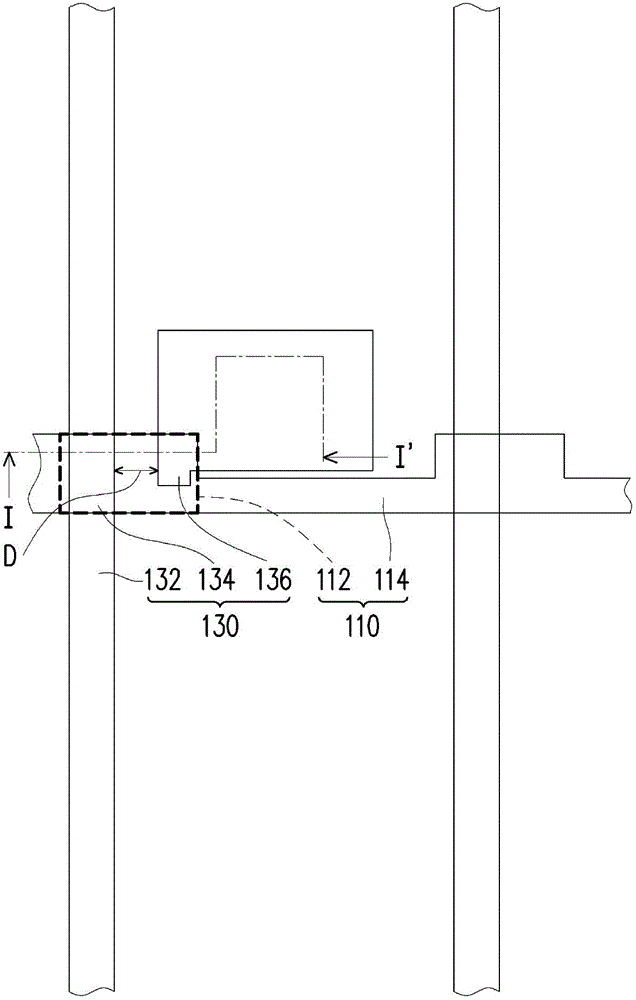
[0039] Figure 1A to Figure 6A It is a schematic top view of the components produced in each step of the method for fabricating the pixel structure according to an embodiment of the present invention, and Figure 1B to Figure 6B respectively Figure 1A to Figure 6A Schematic cross-sectional view along line I-I'. Please refer to Figure 1A and Figure 1B A method for fabricating a pixel structure according to an embodiment of the present invention includes fabricating a patterned conductor layer 110 on a substrate 10 to form a gate 112 to be connected to a scan line 114 . Specifically, the gate 112 formed by the patterned conductive layer 110 and the scan line 114 are formed by a continuous pattern, so the gate 112 can be regarded as a part of the scan line 114 . However, in other embodiments, the patterned conductor layer 110 may include a linear pattern with a fixed line width and a branch pattern connected to the linear pattern, wherein the scan line 114 may be formed by s...


PUM


Abstract

A pixel structure and a method of manufacturing a pixel structure are provided. The pixel structure includes an active device, a gate insulation layer, a dielectric insulation layer, a capacitance electrode, a protection layer and a pixel electrode. The active device includes a gate, a semiconductor channel layer, a source and a drain. The dielectric insulation layer covers the semiconductor channel layer. A dielectric index of the dielectric insulation layer is greater than a dielectric index of the gate insulation layer. The capacitance electrode is overlapped with the drain. The capacitance electrode, the drain and the dielectric insulation layer between the two constitute a storage capacitor structure. The protection layer is disposed on the dielectric insulation layer and the capacitance electrode is located between the protection layer and the dielectric insulation layer. The pixel electrode is disposed on the protection layer and connected to the drain of the active device.

Description

technical field [0001] The present invention relates to a pixel structure and its manufacturing method, and in particular to a high aperture ratio pixel structure and its manufacturing method. Background technique [0002] Currently common flat panel displays use a pixel structure to constitute the smallest basic unit required for displaying images, wherein the pixel structure roughly includes an active element and a pixel electrode. Generally speaking, when the active element in a specific pixel structure is turned on through the corresponding scan line, the operating voltage provided by the data line can be input to the pixel electrode through the active element to display the corresponding display data. In addition, the pixel structure also includes a storage capacitor (storage capacitor), so that the pixel structure has a voltage holding function. That is, the storage capacitor is used to store the operating voltage input to the pixel electrode through the active elemen...

Claims


Application Information

Patent Timeline
Patent Type & Authority Patents(China)
IPC IPC(8): H01L27/02H01L29/786H01L21/77
CPCH01L27/1225H01L27/1248H01L27/1255H01L27/1259H01L29/22H01L29/24H01L29/42356H01L29/66742H01L29/66969H01L29/7869
Inventor 张维仁罗婉瑜陈勃学
Owner AU OPTRONICS CORP
Why Eureka
Try Eureka