Thickness detection stability detection method for wafer edge metrology and inspection tools

A technology for edge thickness and detection tools, applied in the field of microelectronics, which can solve the problem of inability to determine the stability of wafer edge thickness

Active Publication Date: 2016-01-27
SHANGHAI HUALI MICROELECTRONICS CORP
View PDF5 Cites 0 Cited by
  • Summary
  • Abstract
  • Description
  • Claims
  • Application Information

AI Technical Summary

Problems solved by technology

The method overcomes the problem that the detection results of circular edge measurement and detection tools in the prior art cannot determine the stability of wafer edge thickness detection

Method used


Image

  • Thickness detection stability detection method for wafer edge metrology and inspection tools

Examples


Embodiment Construction

[0028] The present invention will be further described below in combination with principle diagrams and specific operation examples.

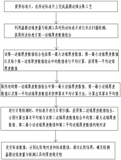
[0029] A method for detecting stability of thickness detection of a wafer edge measurement and detection tool, comprising the following steps:

[0030] S1: Provide a standard sheet and complete the wafer edge removal process on the standard sheet. Specifically, this step can be decomposed into the following steps:

[0031] providing a wafer as a substrate;

[0032] A layer of metal copper film is grown on the wafer;

[0033] Perform a wafer edge removal process on the edge of the exposed wafer to remove the photoresist on the edge of the wafer. Specifically, remove the redundant copper metal on the edge of the wafer with a copper metal film. Specifically, a metal edge washing process or Metal edge etch process removal.

[0034] S2: Use the wafer edge measurement and detection tool to perform multiple scans on the standard wafer to obtain the...


PUM


Abstract

The invention discloses a thickness and stability detection method of a wafer edge measuring and detection tool, wherein the method comprises the following steps that a wafer edge removing process is completed on a standard piece; the standard piece is scanned and detected for a plurality of times through the wafer edge measuring and detection tool, and a first value combination is worked out and comprises a first maximum value and a first value; the mean value of the first value combination is respectively calculated, and a first mean value of each combination is worked out; an arithmetic mean value is calculated through the first maximum value, a first minimum value and the first mean value; daily scanning is carried out to the standard piece, a second value combination is worked out, and the absolute difference between the arithmetic mean value and a second maximum value, a second minimum value and a second mean value in the second value combination is respectively calculated; and a standard value is set, and the absolute difference and the standard value are respectively compared. According to the thickness and stability detection method of the wafer edge measuring and detection tool, the stability and the precision for a machine to detect edge bead rinse (EBR) / wafer edge exposure (WEE) can be detected more intuitively through the deviation.

Description

technical field [0001] The invention relates to the field of microelectronics, in particular to a thickness detection stability detection method of a wafer edge measurement and detection tool. Background technique [0002] With the development of integrated circuit technology and the continuous improvement of machine performance, more and more attention is paid to the defects at the edge of the wafer. Utilizing wafer edge metrology and inspection tools, for example, the CV300R, through wafer edge metrology, is designed to help semiconductor fabs identify wafer edge profile shapes and edge irregularities of films placed on wafers that may impact yield. In implementation, it is a fast and effective quality monitoring method for process steps to detect defects on the wafer edge after EBR (Edge Bead Remover, edge removal process) & WEE (wafer edge expose, wafer edge removal process) by the inspection machine. Therefore, it is very important to ensure the stability and accuracy ...

Claims


Application Information

Patent Timeline
Patent Type & Authority Patents(China)
IPC IPC(8): G01B21/08
Inventor 朱陆君倪棋梁陈宏璘
Owner SHANGHAI HUALI MICROELECTRONICS CORP
Why Eureka
Try Eureka