
UBM etching methods for eliminating undercut

A technology of substrate and copper seed layer, applied in the field of UBM etching, can solve the problems of low yield of manufacturing process and so on

Active Publication Date: 2013-01-09
TAIWAN SEMICON MFG CO LTD
View PDF6 Cites 6 Cited by
  • Summary
  • Abstract
  • Description
  • Claims
  • Application Information

AI Technical Summary

Problems solved by technology

As a result, the metal bumps are delaminated from the corresponding chips or wafers, resulting in low yield of the metal bump manufacturing process

Method used


Image

  • UBM etching methods for eliminating undercut
  • UBM etching methods for eliminating undercut
  • UBM etching methods for eliminating undercut

Examples


Embodiment Construction

[0018] The making and using of various embodiments of the invention are discussed in detail below. It should be appreciated, however, that the present invention provides many applicable concepts that can be implemented in a wide variety of specific contexts. The specific embodiments discussed are illustrative only, and do not limit the scope of the invention.

[0019] According to various aspects of the embodiments, methods of forming undercut-free metal bumps in an underlying underbump metallurgy (UBM) are presented. Metal bumps and intermediate fabrication stages of the UBM are shown according to an embodiment. Modifications of the embodiments are discussed. Like reference numerals are used to refer to like elements throughout the various views and illustrative embodiments.

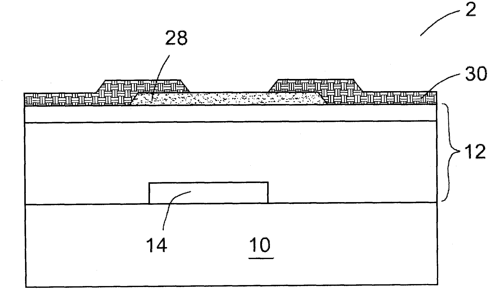
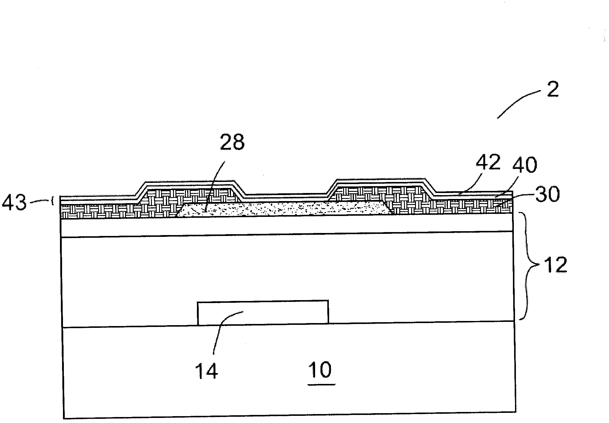
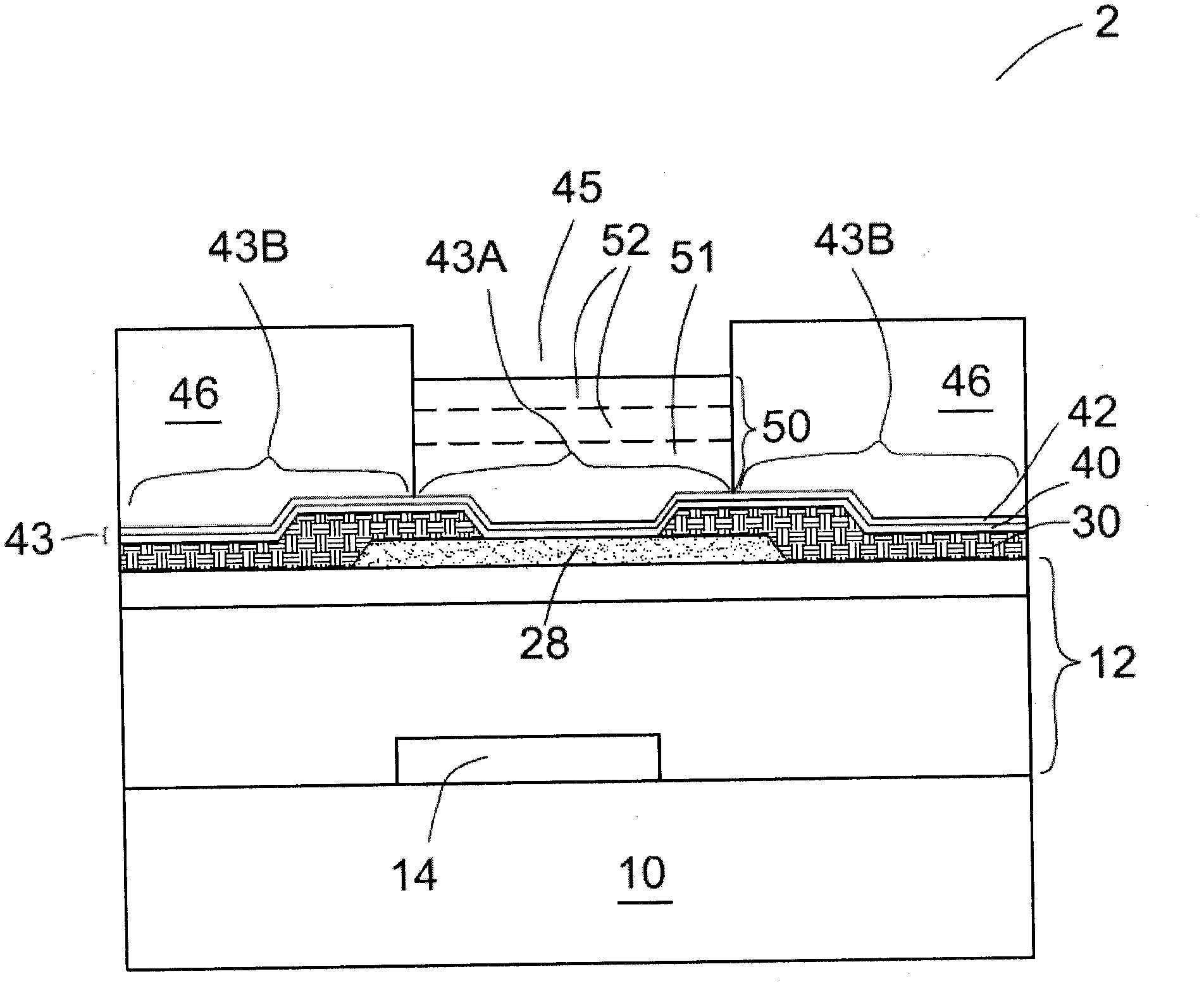
[0020] refer to figure 1 , a wafer 2 comprising a substrate 10 is provided. In an embodiment, the substrate 10 is a semiconductor substrate such as a silicon substrate, however, the substrate may ...


PUM


Abstract

A method includes forming an under-bump metallurgy (UBM) layer overlying a substrate, and forming a mask overlying the UBM layer. The mask covers a first portion of the UBM layer, and a second portion of the UBM layer is exposed through an opening in the mask. A metal bump is formed in the opening and on the second portion of the UBM layer. The mask is then removed. A laser removal is performed to remove a part of the first portion of the UBM layer and to form an UBM.

Description

technical field [0001] The present invention generally relates to the technical field of semiconductors, and more specifically, relates to a UBM etching method. Background technique [0002] In forming a semiconductor wafer, integrated circuit devices, such as transistors, are first formed on the surface of a semiconductor substrate. An interconnect structure is then formed over the integrated circuit device. Metal bumps are formed on the surface of the semiconductor chip to contact the semiconductor circuit device. [0003] In a typical metal bump formation process, an under bump metallurgy (UBM) layer is first formed to electrically connect the metal pads. The UBM layer may include a titanium layer and a copper seed layer over the titanium layer. Metal bumps are then formed (eg, by electroplating) on ​​the UBM layer. The forming process includes forming a mask to cover a first portion of the UBM layer and leave a second portion of the UBM layer uncovered. Metal bumps ...

Claims


Application Information

Patent Timeline
Patent Type & Authority Applications(China)
IPC IPC(8): H01L21/48H01L23/498
CPCH01L2224/13082H01L2224/11464H01L2224/13164H01L2224/11424H01L2224/13007H01L2224/05155H01L2224/05027H01L2224/03632H01L2224/13144H01L2924/01029H01L2224/13147H01L2224/036H01L2224/1147H01L2224/05564H01L2224/05181H01L24/11H01L2224/13083H01L2224/05139H01L2224/0508H01L2224/05572H01L2224/0345H01L24/03H01L2224/05186H01L2224/05124H01L24/05H01L2224/13155H01L24/13H01L2224/13139H01L2224/05166H01L2224/05647H01L2224/05144H01L2224/05022H01L2224/05147H01L2224/11462H01L2224/13111H01L2924/00014H01L2224/0401H01L2924/12042H01L2924/04941H01L2924/04953H01L2924/014H01L2924/01047H01L2924/00012H01L2224/05552H01L2924/00
Inventor 雷弋易郭宏瑞刘重希李明机余振华
Owner TAIWAN SEMICON MFG CO LTD
Learn More