Package structure and method for fabricating the same

A technology of packaging structure and manufacturing method, which is applied in semiconductor/solid-state device manufacturing, electrical components, electric solid-state devices, etc., can solve the problems of poor electrical connection of packaging structure, achieve good electrical performance, and shorten the wiring length.

Inactive Publication Date: 2013-01-09
MEDIATEK INC
View PDF3 Cites 4 Cited by
  • Summary
  • Abstract
  • Description
  • Claims
  • Application Information

AI Technical Summary

Problems solved by technology

[0007] In order to solve the technical problem of poor electrical connection of the above packaging structure, the present invention provides a new packaging structure

Method used


Image

  • Package structure and method for fabricating the same
  • Package structure and method for fabricating the same
  • Package structure and method for fabricating the same

Examples


Embodiment Construction

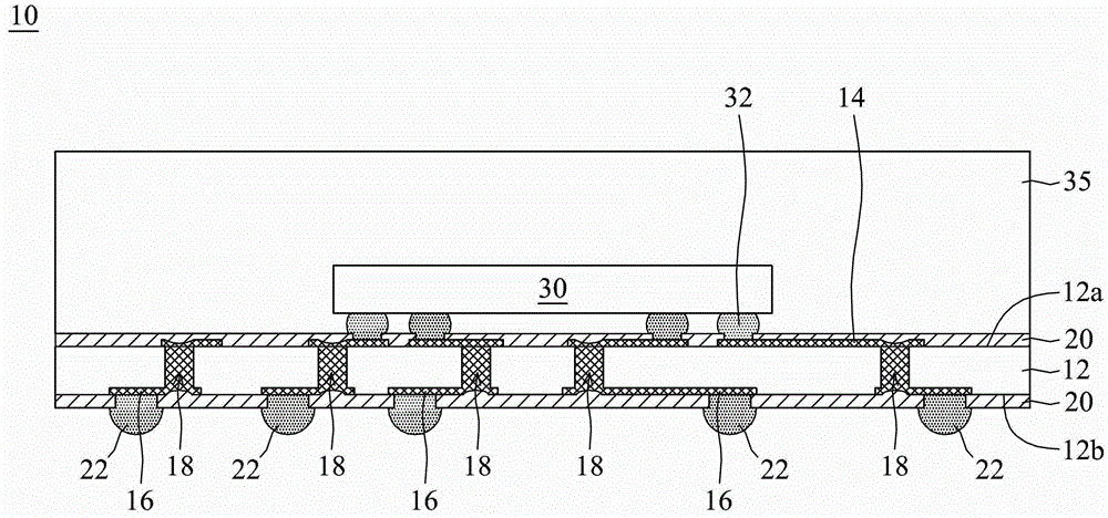
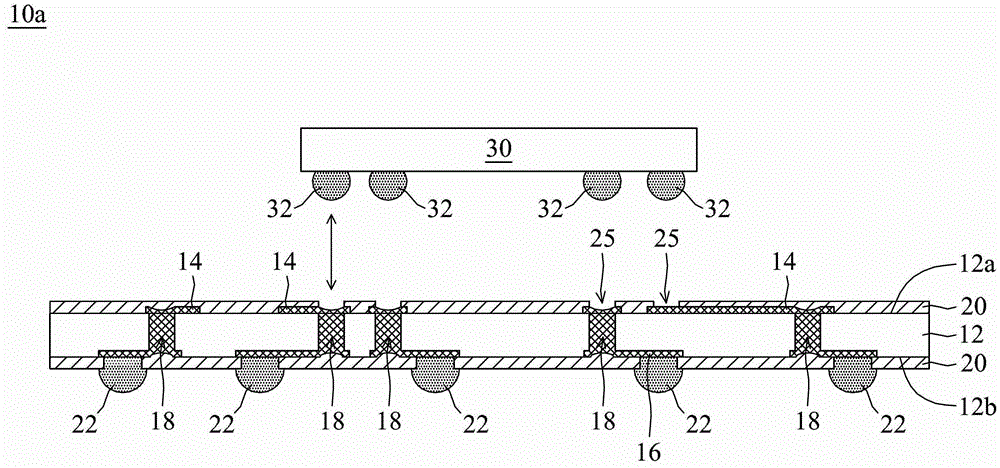
[0015] Certain terms are used in the description and claims to refer to particular components. Those skilled in the art should understand that hardware manufacturers may use different terms to refer to the same component. The specification and claims do not use the difference in name as a way to distinguish components, but use the difference in function of components as a criterion for distinguishing. The "comprising" mentioned throughout the specification and claims is an open term, so it should be interpreted as "including but not limited to". In addition, the term "coupled" herein includes any direct and indirect means of electrical connection. Therefore, if it is described that the first device is coupled to the second device, it means that the first device may be directly electrically connected to the second device, or indirectly electrically connected to the second device through other devices or connection means.

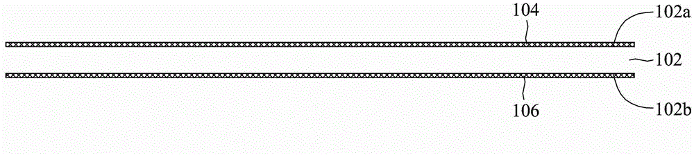
[0016] See Figure 3A Firstly, a substrate 102 is pr...


PUM


Abstract

The invention provides a package structure and a method for fabricating the same. The package structure includes a substrate, wherein the substrate has a first surface and a second surface, and a first pattern metal layer is formed on the first surface, and a second patterned metal layer is formed on the second surface, and the substrate has a plurality of vias formed therein, wherein the first patterned metal layer is electrically connected to the second patterned metal layer through the plurality of vias, and the widths of the plurality of vias are gradually increased from the first surface to the second surface; a chip formed on the first surface of the substrate; and a molding material is formed on the substrate and the chip, wherein the chip is covered by the molding material. According to the invention, better electric performances can be obtained.

Description

technical field [0001] The present invention relates to a packaging structure, and in particular to a packaging structure in which bumps on a chip are located above through holes and a manufacturing method thereof. Background technique [0002] With the vigorous development of the electronic industry, electronic products are constantly pursuing lightness, thinness and compactness, which makes integrated circuits (Integrated Circuit, IC) also develop towards high integration and miniaturization. [0003] figure 1 A cross-sectional view of a conventional packaging structure 10 is shown. The packaging structure 10 includes a substrate 12 ; a chip 30 is formed on the substrate 12 ; and a packaging material 35 is formed on the substrate 12 and the chip 30 . The substrate 12 has a first surface 12a and a second surface 12b, the first surface 12a has a first patterned metal layer (patterned metal layer) 14, the second surface 12b has a second patterned metal layer 16, and the subs...

Claims


Application Information

Patent Timeline
Patent Type & Authority Applications(China)
IPC IPC(8): H01L23/498H01L21/60H01L23/31H01L21/56
CPCH01L21/486H01L2224/13082H01L23/49894H01L2224/13164H01L23/49827H01L23/49816H01L2224/16237H01L24/81H01L2224/13155H01L24/13H01L2224/16235H01L2224/13144H01L2924/15311H01L23/3128H01L2224/13147H01L2224/131H01L24/16H01L2224/16225H01L2924/12042H01L2924/00014H01L2924/014H01L2924/00
Inventor 谢东宪
Owner MEDIATEK INC
Why Eureka
Try Eureka