
Seamlessly spliced photoelectronic imaging system with double lens using 25 area-array detectors

A technology of area array detectors and imaging systems, which is applied to the parts of TV systems, TVs, instruments, etc., can solve the problems of long working distance, movement mechanism, reliability and long-term stability of system accuracy, etc., to achieve The structure is simple and easy to implement, the system accuracy is stable and reliable, and there is no effect of motion mechanism

Inactive Publication Date: 2013-01-16
INST OF OPTICS & ELECTRONICS - CHINESE ACAD OF SCI
View PDF6 Cites 12 Cited by
  • Summary
  • Abstract
  • Description
  • Claims
  • Application Information

AI Technical Summary

Problems solved by technology

There are deficiencies in the long-term stability of the motion mechanism, reliability, and system accuracy, and the long working distance behind

Method used


Image

  • Seamlessly spliced photoelectronic imaging system with double lens using 25 area-array detectors
  • Seamlessly spliced photoelectronic imaging system with double lens using 25 area-array detectors
  • Seamlessly spliced photoelectronic imaging system with double lens using 25 area-array detectors

Examples


Embodiment Construction

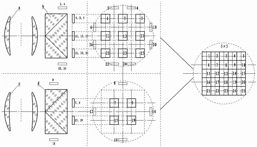
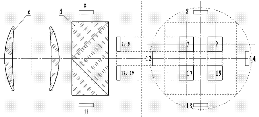
[0030] like figure 1 As shown, the present invention includes 2 sets of imaging systems. The first set of imaging systems includes the first lens a, beam splitting prism b, and 17 pieces of area array detectors; the second set of imaging systems includes lens c, beam splitting prism d, and 8 pieces of area array detectors. Group; combined to realize the image plane seamless splicing imaging photoelectric system of 25 area array detectors.

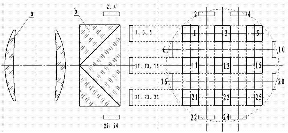
[0031] like figure 2 As shown in the figure, a beam splitter prism b and 17 area array detectors are placed behind lens a, of which 9 area array detectors are placed on the main image plane, and 2 area array detectors are placed on each of the 4 side image planes. The area array detectors placed on the main image plane are 1, 3, 5, 11, 13, 15, 21, 23, 25. Area array detectors 2, 4, 6, 10, 16, 20, 22, and 24 are placed on the side image plane; when viewed from the lens to the main image plane, area array detectors 2 and 4 are located on t...


PUM


Abstract

The invention discloses a seamlessly spliced photoelectronic imaging system with double lens using 25 area-array detectors. The photoelectronic imaging system is characterized in that a structure of two imaging systems and a prism beam splitting way are adopted; on a first lens, imaging of 17 area-array detectors is realized, wherein 9 area-array detectors are disposed on a main image surface, and 8 area-array detectors are disposed on four lateral image surfaces, specifically, 2 area-array detectors are disposed on each of the four lateral image surfaces respectively; on a second lens, imaging of 8 area-array detectors is realized, wherein 4 area-array detectors are disposed on a main image surface, and 4 area-array detectors are disposed on four lateral image surfaces, specifically, 1 area-array detector is disposed on each of the four lateral image surfaces respectively; the two imaging systems and the area-array detectors are combined to realize seamless splicing of the image surfaces which are formed by 25 area-array detectors in a 5*5 mode; a beam splitting prism is realized through combination of one rectangular pyramid mirror and four semi-rectangular pyramid mirrors; beam splitting on a beam splitting surface is realized by adopting half-transmission and half-reflection, so that equal-energy beam splitting is realized, and splicing vignetting of the area-array detectors is eliminated. The system disclosed by the invention can be applied to aeronautic and astronautic optical imaging and optical detection instruments and equipment, and is particularly suitable for aeronautic and astronautic surveying and mapping cameras with large fields of view and using ultra-large area-array detectors.

Description

technical field [0001] The invention belongs to a seamless imaging photoelectric system spliced ​​with super large area array detectors, in particular to a seamless splicing imaging photoelectric system with double lenses and 25 area array detectors. Background technique [0002] With the development of aviation and aerospace technology, the demand for photoelectric imaging systems with large area arrays and ultra-large area arrays is becoming more and more urgent. Two methods are often used to achieve large-scale array imaging. One is to customize ultra-large-scale detector devices at detector manufacturers, and the other is to use detector splicing. [0003] At present, the scale of single-chip large area array detectors in the world is about 17k×15k (DMC250), which is not a commodity on the shelf, and the application cost is expensive. In addition, further increasing the scale of single-chip detectors is also a technical bottleneck in the development of current detectors...

Claims


Application Information

Patent Timeline
IPC IPC(8): H04N5/225G02B27/10H01L25/065
Inventor 梁伟王甲峰高晓东庄富强
Owner INST OF OPTICS & ELECTRONICS - CHINESE ACAD OF SCI
Learn More