Film defect inspection device, defect inspection method, and release film
A defect inspection and inspection device technology, applied in measurement devices, optical testing of flaws/defects, material analysis by optical means, etc., can solve the problems of small contrast difference, difficulty in inspection, and inability to inspect films, and achieve a high contrast ratio. Effect
- Summary
- Abstract
- Description
- Claims
- Application Information
AI Technical Summary
Problems solved by technology
Method used
Image

Examples
Embodiment 1
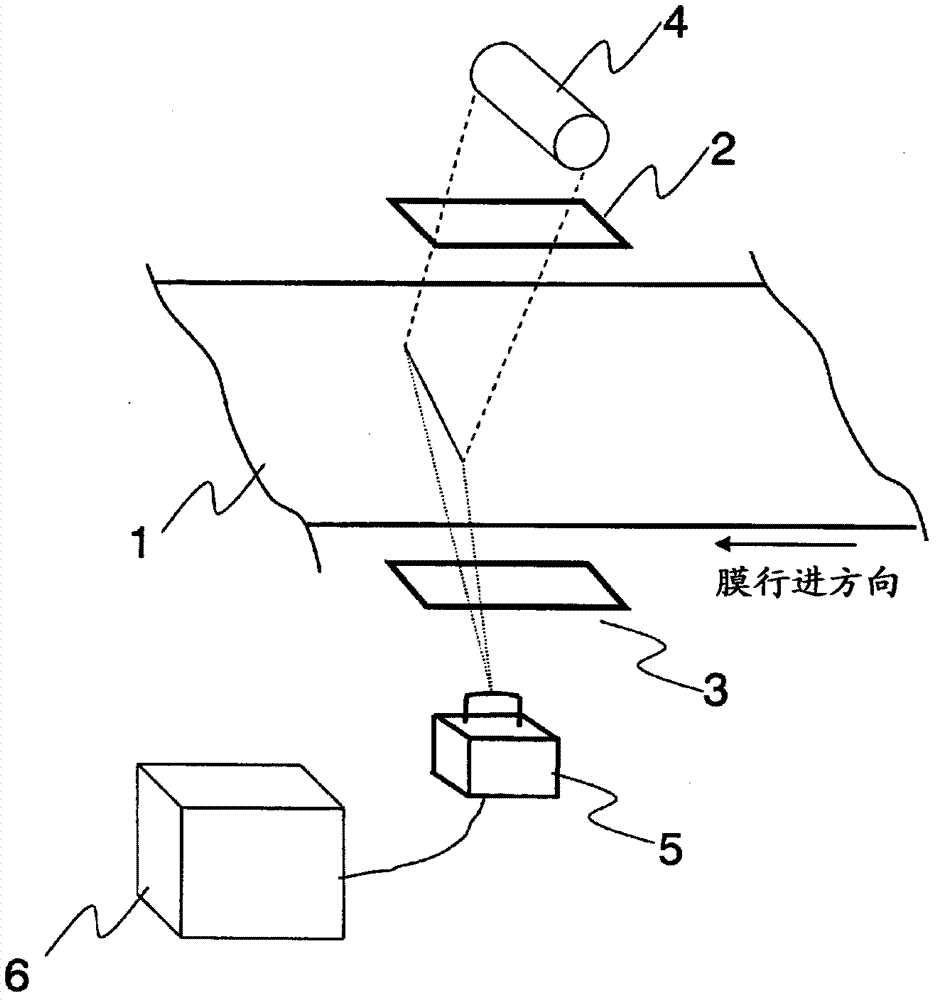
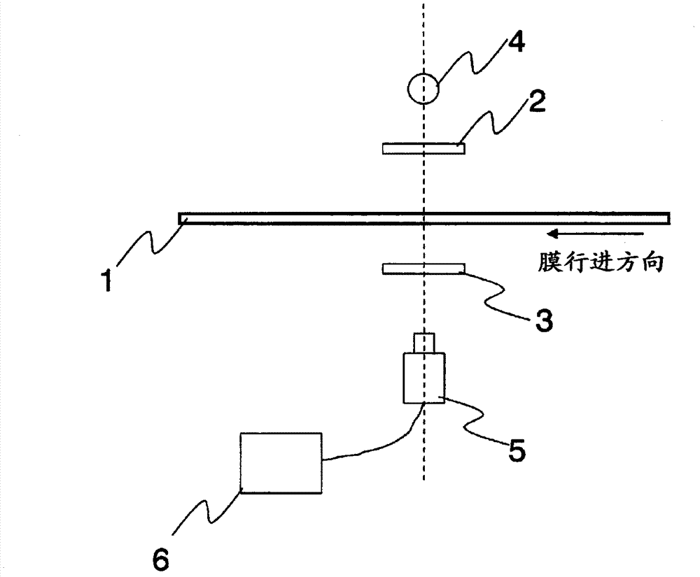
[0066] As a sample to be inspected, "Lumiror" [38R64] manufactured by Toray was prepared.
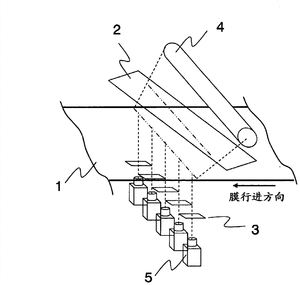
[0067] In the defect inspection device of the present invention, a 250W metal halide (BMH-250A manufactured by Mejiro Precision) was used as an illumination mechanism, and a CCD camera (P3-80-8K manufactured by DALSA) with a resolution of 25 μm was used as a light receiving mechanism. -40) and the second polarizing plate are combined and arranged in multiples, and the test sample is imaged at an inspection width of 1255 mm to check the base light receiving amount.
[0068] In the evaluation of the basic received light quantity, adjust the angles of both the first polarizer and the second polarizer, and check the maximum value and the minimum value of the received light quantity in the state where the average value of the received light quantity over the entire inspection width is the smallest when evaluated in 256 grayscale. The difference in value was evaluated as a difference in recei...
PUM
 Abstract
Description
Claims
Application Information
 - R&D
- Intellectual Property
- Life Sciences
- Materials
- Tech Scout
- Unparalleled Data Quality
- Higher Quality Content
- 60% Fewer Hallucinations
Browse by: Latest US Patents, China's latest patents, Technical Efficacy Thesaurus, Application Domain, Technology Topic, Popular Technical Reports.
© 2025 PatSnap. All rights reserved.Legal|Privacy policy|Modern Slavery Act Transparency Statement|Sitemap|About US| Contact US: help@patsnap.com