Array substrate, manufacturing method thereof, and display device
An array substrate and manufacturing method technology, applied in the field of liquid crystal display, can solve problems such as electrostatic breakdown and easy accumulation of charges, and achieve the effect of increasing common electrode resistance and reducing electrostatic breakdown
- Summary
- Abstract
- Description
- Claims
- Application Information
AI Technical Summary
Problems solved by technology
Method used
Image
Examples
Embodiment 1
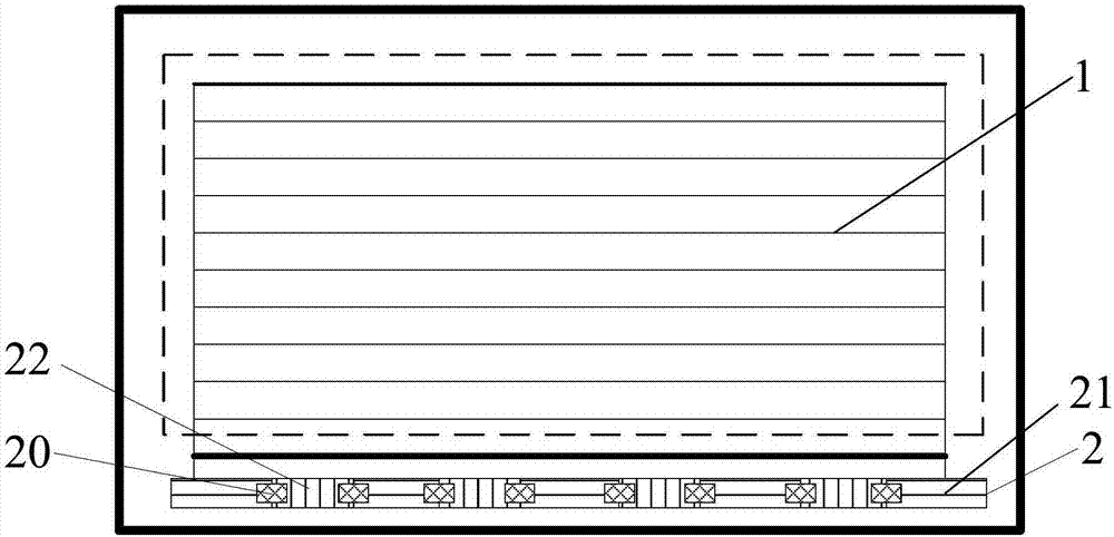
[0036] This embodiment provides an array substrate, such as figure 2 and image 3 As shown, it includes a common electrode bus 2 and a plurality of parallel common electrode lines 1, wherein the common electrode bus 2 is located outside the effective display area, the common electrode line 1 is located inside the effective display area, and the plurality of parallel common electrode lines 1 connected together in parallel. The common electrode bus 2 in this embodiment includes a plurality of spaced gate metal segments 21 and a plurality of spaced source-drain metal segments 22, and the source-drain metal segments 22 correspond to the gaps between the gate metal segments 21. The vacant position of the gate metal segment 21 is separated from the source-drain metal segment 22 by the first insulating layer 3. As an embodiment of the present invention, the first insulating layer 3 may be a gate Insulation. Preferably, the gate metal segment 21 and the source-drain metal segment ...
Embodiment 2
[0056] This embodiment provides an array substrate, such as figure 2 As shown, it includes a common electrode bus 2 and a plurality of parallel common electrode lines 1, wherein the common electrode bus 2 is located outside the effective display area, the common electrode line 1 is located inside the effective display area, and the plurality of parallel common electrode lines 1 connected together in parallel. The common electrode bus 2 in this embodiment includes a plurality of spaced gate metal segments 21 and a plurality of spaced source-drain metal segments 22, and the source-drain metal segments 22 correspond to the gaps between the gate metal segments 21. The vacant position of the gate metal segment 21 is separated from the source-drain metal segment 22 by the first insulating layer 3. As an embodiment of the present invention, the first insulating layer 3 may be a gate insulating layer. Preferably, the gate metal segment 21 and the source-drain metal segment 22 have ...
PUM
 Abstract
Description
Claims
Application Information


