A kind of array substrate and display panel

A technology for array substrates and display panels, which is used in semiconductor/solid-state device parts, semiconductor devices, electrical components, etc., can solve the problems of high product defect rate, the inability of array substrates to eliminate accumulated electrostatic charges, product defects, etc. The effect of electrostatic capacity, reduction of electrostatic breakdown, and reduction of replacement frequency

Active Publication Date: 2022-01-07
SHANGHAI AVIC OPTOELECTRONICS
View PDF0 Cites 0 Cited by
  • Summary
  • Abstract
  • Description
  • Claims
  • Application Information

AI Technical Summary

Problems solved by technology

[0003] Because there is no static electricity removal equipment in a vacuum environment, when static electricity accumulates, the array substrate will not be able to eliminate the accumulated static electricity charge, especially on the isolated electrodes and data lines of sub-pixels. Please refer to figure 1 , because the drain 01 electrically connected to the pixel electrode is a pointed structure, resulting in a large amount of charge accumulation at the pointed structure
However, a large amount of charge accumulated at the tip structure will cause discharge between the tip structure and the adjacent data line 02 or gate line 03, resulting in a large number of defective products.
Moreover, as the sub-pixel area increases, the above-mentioned discharge phenomenon will become more intense, and the defective rate of the product will be higher.

Method used


Image

  • A kind of array substrate and display panel
  • A kind of array substrate and display panel
  • A kind of array substrate and display panel

Examples


Embodiment approach

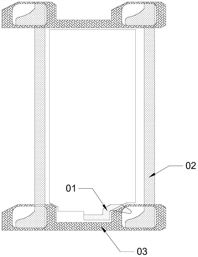
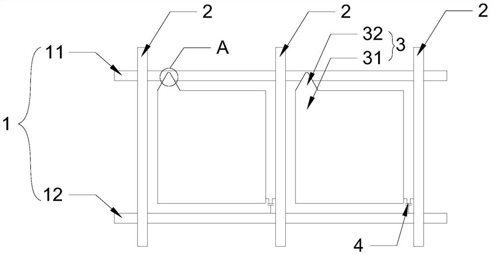
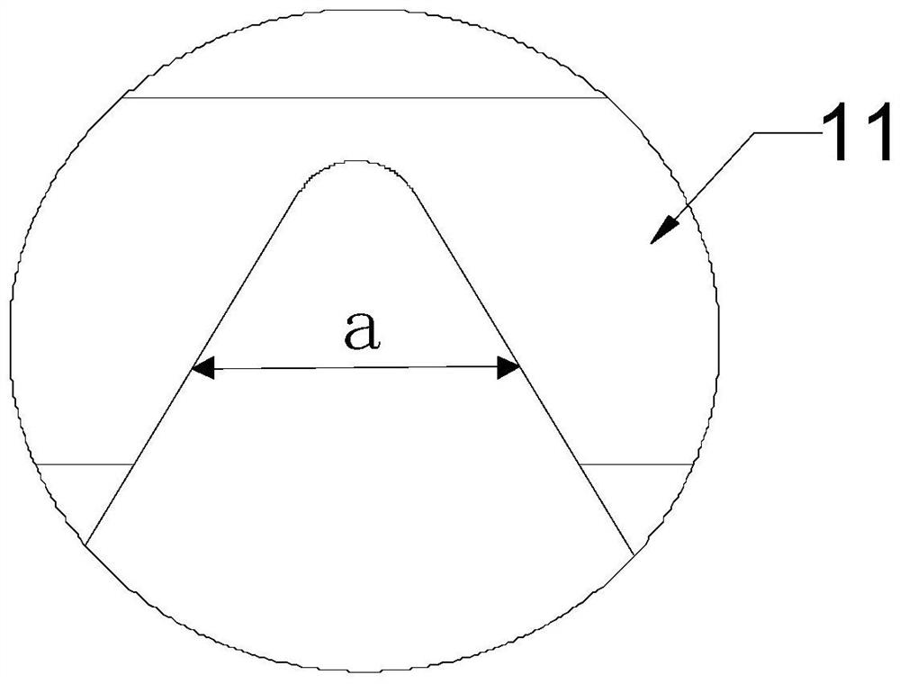
[0056] Way 1: In the first direction, the width of the protruding portion 32 in the first region is less than or equal to 8 μm, and each repeating unit includes a sub-pixel unit, and in each sub-pixel unit:

[0057] A first gate line 11 and a second gate line 12 connected to the transistor 4 are formed on both sides of the pixel electrode 3, and along the second direction, at least one protrusion 32 is located on the side of the pixel electrode 3 facing the first gate line 11 , and the vertical projection of the protrusion 32 on the substrate overlaps with the vertical projection of the first grid line 11 on the substrate, such as figure 2 As shown, the number of protrusions 32 on each pixel electrode 3 can be one, or, as Figure 4 As shown, the number of protrusions 32 on each pixel electrode 3 can be two, of course, the number of protrusions 32 on each pixel electrode 3 can also be set to other numbers, which will not be repeated here.

[0058] It should be noted that sinc...


PUM

PropertyMeasurementUnit
widthaaaaaaaaaa

Abstract

The present invention relates to the field of display technology, and discloses an array substrate and a display panel. The array substrate includes: a substrate, gate lines formed on the substrate, data lines, pixel electrodes, and transistors electrically connected to the pixel electrodes, wherein: The pixel electrode includes a main body and at least one protrusion, the protrusion includes a first region, and in the first direction and / or the second direction, the width of the protrusion in the first region is less than or equal to 8 μm; the first direction and the gate line The extension directions of the data lines are the same, and the second direction is the same as the extension direction of the data lines. The array substrate provided by the present invention is provided with protrusions at the pixel electrodes, through which the electrostatic charge accumulated by the transistor can be derived, thereby better improving the antistatic ability of the product, reducing the occurrence of electrostatic breakdown, and reducing the induction of static electricity related equipment spare parts Replacement frequency of spare parts reduces production costs.

Description

technical field [0001] The present invention relates to the field of display technology, in particular to an array substrate and a display panel. Background technique [0002] A large amount of static electricity is generated during the manufacture and transfer of existing array substrates in vacuum equipment. [0003] Because there is no static electricity removal equipment in a vacuum environment, when static electricity accumulates, the array substrate will not be able to eliminate the accumulated static electricity charge, especially on the isolated electrodes and data lines of sub-pixels. Please refer to figure 1 , because the drain 01 electrically connected to the pixel electrode is a pointed structure, resulting in a large amount of charge accumulated at the pointed structure. However, a large amount of charges accumulated at the tip structure will cause discharge between the tip structure and the adjacent data line 02 or gate line 03 , resulting in a large number of...

Claims


Application Information

Patent Timeline
Patent Type & Authority Patents(China)
IPC IPC(8): H01L27/12H01L23/60
CPCH01L23/60H01L27/124H01L27/1237
Inventor 严茂程
Owner SHANGHAI AVIC OPTOELECTRONICS
Why Eureka
Try Eureka