Array substrates, display devices, electronic devices

An array substrate and pre-charging technology, which is applied in the direction of instruments, nonlinear optics, optics, etc., can solve the problems of affecting the display effect and reducing the aperture ratio of the display panel, and achieve the effect of solving insufficient charging

Active Publication Date: 2015-12-02
BOE TECH GRP CO LTD +1
View PDF6 Cites 0 Cited by
  • Summary
  • Abstract
  • Description
  • Claims
  • Application Information

AI Technical Summary

Problems solved by technology

However, the increase of the W / L of the channel will cause a decrease in the aperture ratio of the display panel, which will affect the display effect.

Method used


Image

  • Array substrates, display devices, electronic devices
  • Array substrates, display devices, electronic devices
  • Array substrates, display devices, electronic devices

Examples


Embodiment 1

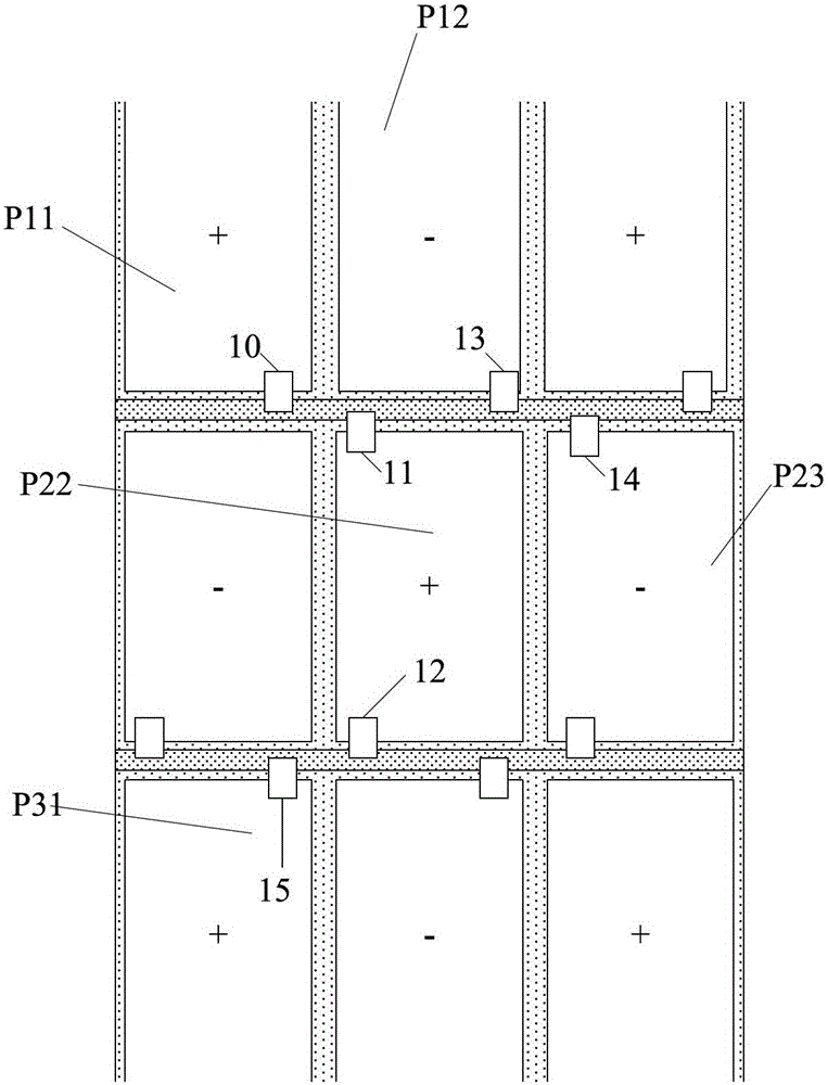
[0027] Such as figure 1 Shown is the pixel structure of the array substrate of this embodiment, from figure 1 It can be seen that in the same row of sub-pixels on the array substrate, the polarities of adjacent sub-pixels are opposite; in the same row of sub-pixels on the array substrate, the polarities of adjacent sub-pixels are opposite.

[0028] for figure 1 For the sub-pixel P22 in the middle, it includes a charging TFT12 electrically connected to the scanning line corresponding to the sub-pixel in this row and a pixel electrode corresponding to the charging TFT12, wherein the sub-pixel P22 also includes a pre-charging TFT11 and a pre-charging TFT11. Corresponding to the pixel electrode, the pre-charging TFT 11 is electrically connected to the scanning line corresponding to the sub-pixel in the upper row.

[0029] Depend on figure 1 It can be seen that the sub-pixel P11 is located in the upper row of the sub-pixel P22, and has the same polarity as the sub-pixel P22, so ...

Embodiment 2

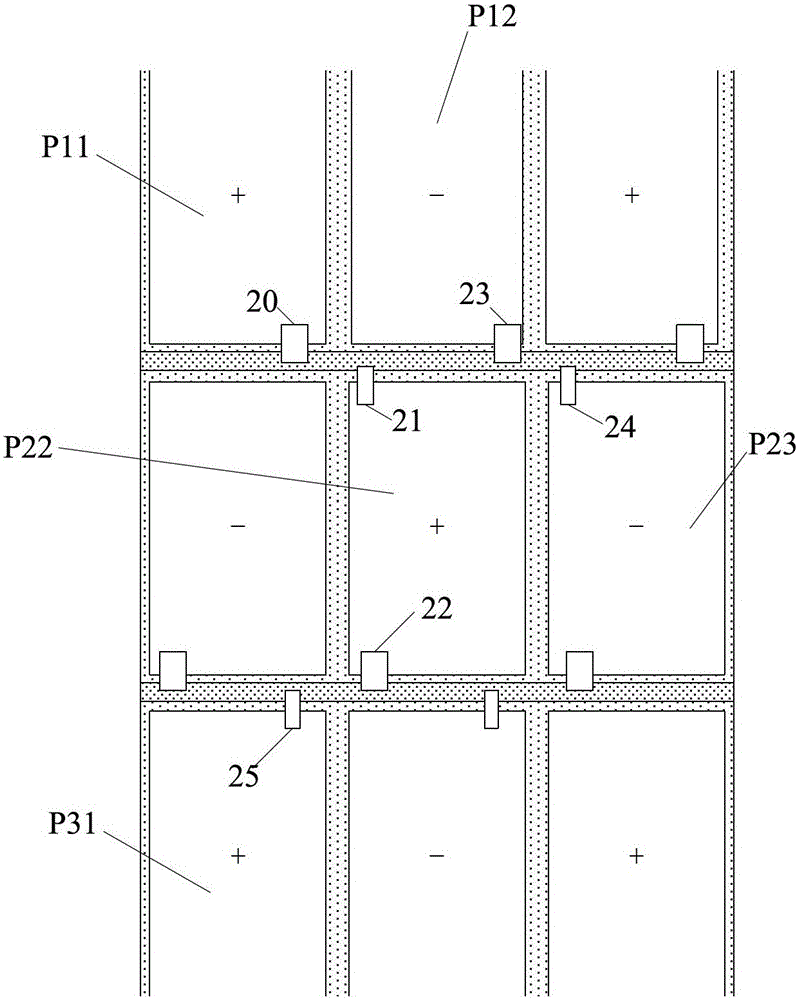
[0036] Such as figure 2 Shown is the pixel structure of the array substrate of this embodiment, from figure 2 It can be seen that in the same row of sub-pixels on the array substrate, the polarities of adjacent sub-pixels are opposite; in the same row of sub-pixels on the array substrate, the polarities of adjacent sub-pixels are opposite.

[0037] for figure 2 For the sub-pixel P22 in the middle, it includes a charging TFT22 electrically connected to the scanning line corresponding to the sub-pixel in this row and a pixel electrode corresponding to the charging TFT22, wherein the sub-pixel P22 also includes a pre-charging TFT21 and a charging TFT connected to the pre-charging TFT21. Corresponding to the pixel electrode, the pre-charging TFT 21 is electrically connected to the scanning line corresponding to the sub-pixel in the upper row.

[0038] Depend on figure 2It can be seen that the sub-pixel P11 is located in the upper row of the sub-pixel P22, and has the same p...

Embodiment 3

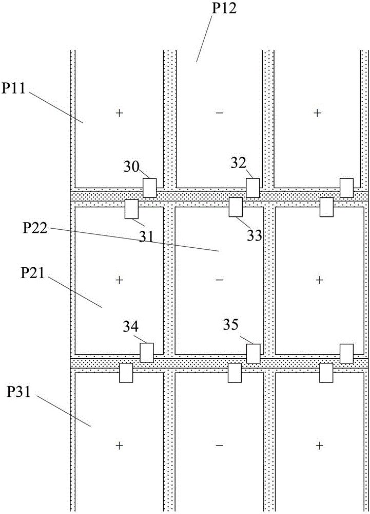
[0045] Such as image 3 Shown is the pixel structure of the array substrate of this embodiment, from image 3 It can be seen that in the same row of sub-pixels on the array substrate, the polarities of adjacent sub-pixels are opposite; in the same row of sub-pixels on the array substrate, the polarities of adjacent sub-pixels are the same.

[0046] for image 3 For the sub-pixel P22 in the middle, it includes a charging TFT35 electrically connected to the scanning line corresponding to the sub-pixel in this row and a pixel electrode corresponding to the charging TFT35, wherein the sub-pixel P22 also includes a pre-charging TFT33 and a charging TFT33 Corresponding to the pixel electrode, the pre-charge TFT 33 is electrically connected to the scanning line corresponding to the sub-pixel in the upper row.

[0047] Depend on image 3 It can be seen that the sub-pixel P12 is located in the upper row of the sub-pixel P22, and has the same polarity as the sub-pixel P22, so that wh...


PUM


Abstract

The invention provides an array substrate, a display device and an electronic device, belonging to the display field. The array substrate is provided with a plurality of sub pixels arranged into a matrix, a plurality of scanning lines and a plurality of data lines, one scanning line is arranged between the two adjacent rows of sub pixels, each row of sub pixels correspond to one scanning line, each sub pixel comprises a charging TFT (thin-film transistor) electrically connected with the scanning line corresponding to the row of sub pixels, and a pixel electrode corresponding to the charging TFT, wherein each sub pixel further comprises a precharging TFT and a pixel electrode corresponding to the precharging TFT, and the precharging TFT is electrically connected with the scanning line corresponding to the superiorprevious row of sub pixels. According to the technical scheme, the array substrate can meet the charging rate requirement of the sub pixels can be met under the condition of not influencing the display effect.

Description

technical field [0001] The present invention relates to the display field, in particular to an array substrate, a display device, and an electronic device. Background technique [0002] At present, large-size TV products and 3D products are the development trend in the display field. However, in order to realize the development of large-size TV products and 3D products, the problem of shortening the charging time caused by high-frequency driving must be solved. If the driving frequency of the product is increased from 60Hz to 120Hz or even 240Hz, the charging time for each sub-pixel will be shortened to 1 / 2 or even 1 / 4 of the original, which will have a serious impact on the charging rate of the sub-pixel . [0003] At present, in order to ensure the charging rate of the sub-pixel, the usual solution is to increase the W / L (width-to-length ratio) of the channel to increase the charging current value (I on ), so that the target charging rate can be achieved while the chargi...

Claims


Application Information

Patent Timeline
Patent Type & Authority Patents(China)
IPC IPC(8): G02F1/1362G02F1/1368
Inventor 刘莎
Owner BOE TECH GRP CO LTD
Why Eureka
Try Eureka