Power source apparatus for display and image display apparatus

a technology of power source apparatus and display screen, which is applied in the direction of static indicating device, liquid/fluent solid measurement, instruments, etc., can solve the problems of streak display defects on the screen, inability to achieve low power consumption, and more noticeable afterimage problems, so as to prevent the occurrence of afterimages and prevent the latch-up phenomenon. , the effect of low power consumption

Inactive Publication Date: 2010-04-13
SHARP KK
View PDF12 Cites 2 Cited by
  • Summary
  • Abstract
  • Description
  • Claims
  • Application Information

AI Technical Summary

Benefits of technology

[0044]In the power source apparatus for a display according to the present invention, the active element as the switching section is in the OFF state in driving the power source, and therefore, leakage current does not consistently flow through the earth connection terminal (reference potential terminal), thereby realizing low power consumption.
[0045]Further, when the power source is in the OFF state, the active element is in the ON state and constitutes a discharge circuit. Therefore, the power source voltage can be caused to steeply drop while keeping low power consumption, thereby making it possible to discharge electric charges remaining in pixels and prevent occurrence of afterimages. Furthermore, in this case, the active element, or a discharge resistor connected to the active element in series, serves as a current suppressing means, thereby making it possible to prevent the latch-up phenomenon.
[0046]Furthermore, when the power source is in the OFF state, the power source output

Problems solved by technology

This ability makes the above-described afterimage problem more noticeable.
When a power source switch is turned ON or off, streak display defects appear on the screen.
Low power consumption cannot be achieved.
Thus, an attempt to overcome the afterimage problem by steepening the fall of the power source unfortunately leads to an increase in power consumption.
In this case, electric charges are not sufficiently removed from pixels, resulting in an afterimage.
To address the latch-up phenomenon or the like, a diode is provided in an output portion of the liquid crystal driver IC, however it is insufficient.
Specifically, when a main power source falls, the voltage becomes unstable, leading to destruction of the display driver.
Therefore, the period of time for discharging from the pixel (electric charge r

Method used


Image

  • Power source apparatus for display and image display apparatus
  • Power source apparatus for display and image display apparatus
  • Power source apparatus for display and image display apparatus

Examples


embodiment 1

[0071]FIG. 1 is a block diagram showing a liquid crystal display apparatus according to Embodiment 1 of the present invention.

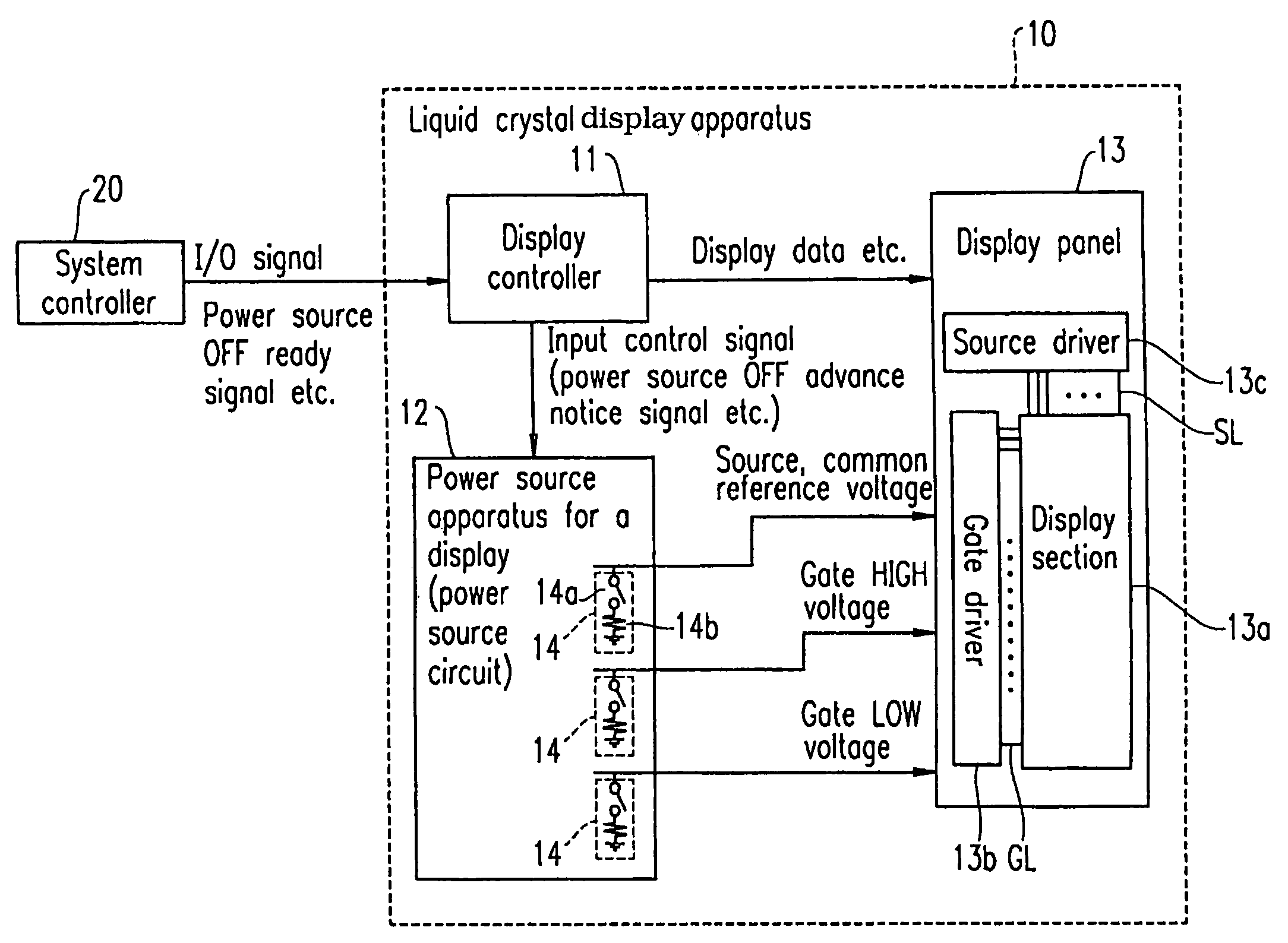
[0072]Referring to FIG. 1, a liquid crystal display apparatus 10 comprises a display controller 11, a power source circuit 12 (power source apparatus for a display), and a display panel 13 having a display section 13a.

[0073]The display controller 11 receives I / O (Input / Output) signals, a power source OFF ready signal and the like output from an external system controller 20 and outputs various signals, such as display data and the like, to the display panel 13 as well as a power source OFF advance notice signal (input control signal) to a power source circuit 12.

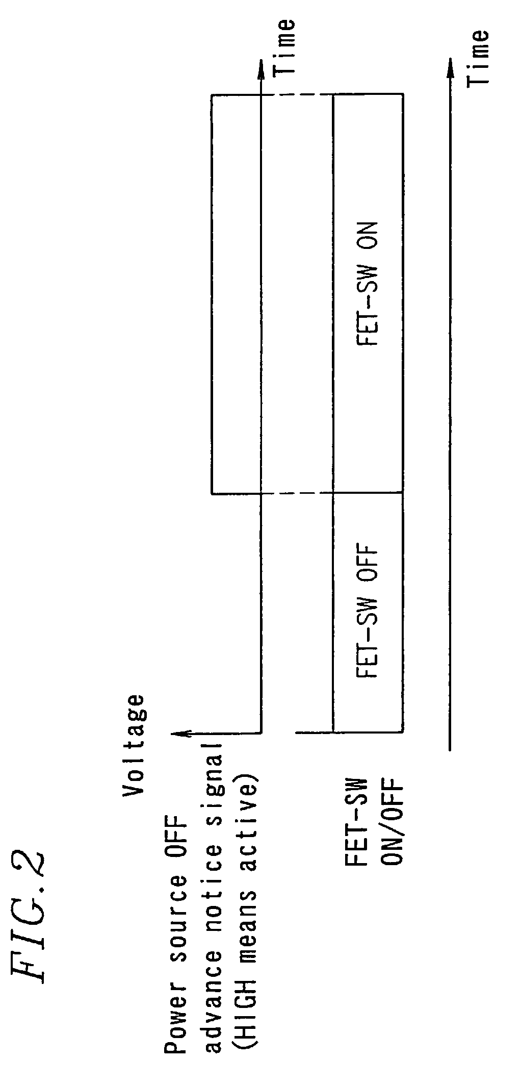
[0074]The power source circuit 12 receives a power source OFF advance notice signal and the like from the display controller 11. The power source circuit 12 has a discharge circuit 14 comprising a FET-SW (switching means comprising a FET transistor) 14a which transitions the ON state to the OFF state...

embodiment 2

[0095]In Embodiment 2, based on a power source OFF ready signal output from the system controller 20, 0 (V) or any constant voltage is applied as a pixel voltage to each pixel in the display panel 13 (mask writing).

[0096]FIG. 7 is a timing chart of signal voltages applied to a display panel 13 of a liquid crystal display apparatus according to Embodiment 2 of the present invention. The signal voltages are applied to the display panel 13 when 0 (V) or any constant voltage is applied as a pixel voltage to each pixel in the display panel 13 (mask writing). FIG. 15 is a block diagram schematically showing a configuration of a liquid crystal display apparatus 10A according to Embodiment 2 of the present invention. Members having substantially the same action and effect as those of FIG. 1 are referenced by the same numerals.

[0097]Referring to FIG. 7, 0 (V) or any constant voltage is applied as a pixel voltage to each pixel in the display panel 13 (mask writing) based on a power source OFF...

embodiment 3

[0105]In Embodiment 3, electric charges remaining in pixels are sufficiently discharged by controlling the mask writing time period and the gate voltage HIGH time period as in Embodiment 2 so that afterimages are overcome. In addition, a resistor element (the resistor element in the Related Art section) is used instead of the FET-SW 14a of Embodiment 1 and 2. FIG. 16 is a block diagram schematically showing a configuration of a liquid crystal display apparatus 10B according to Embodiment 3 of the present invention. Members having substantially the same action and effect as those of FIG. 1 are referenced by the same numerals.

[0106]A display controller 11B performs mask writing by applying a pixel voltage of 0 (V) or a predetermined value to each pixel for one horizontal time period or more based on a predetermined power source OFF ready signal from the system controller 20. Thereafter, the power source supply from the power source circuit 12 to the power source display section 13a is...


PUM


Abstract

A power source apparatus for a display is provided, which comprises a voltage generating section capable of controlling outputting or output termination of one or more predetermined output voltages, and a switching section provided between an output terminal of the predetermined output voltage and a predetermined reference potential terminal. The switch section is turned from OFF to ON when the voltage generating section performs the output termination control.

Description

BACKGROUND OF THE INVENTION[0001]1. Field of the Invention[0002]The present invention relates to a power source apparatus for a display for generating and supplying a predetermined voltage to each section, and an image display apparatus incorporating the same (e.g., a liquid crystal display apparatus and the like).[0003]2. Description of the Related Art[0004]Conventionally, a liquid crystal display apparatus is provided with a display panel comprising a display section. The display section has a plurality of pixels arranged in a matrix. Each pixel is provided with a thin film transistor (TFT). A display signal is applied between the pixel electrode and the common electrode (counter electrode) of each pixel to perform image displaying. Typically, the TFT is formed of a MOSFET having a source electrode, a drain electrode and a gate electrode. The drain electrode of the TFT is connected to the pixel electrode of the pixel. The source electrode of the TFT is connected to a source bus li...

Claims


Application Information

Patent Timeline
IPC IPC(8): G06F1/26G06F1/32G09G3/36
CPCG09G3/3696G09G2330/02G09G2310/0245
Inventor YAMATO, ASAHIYANAGI, TOSHIHIRO
Owner SHARP KK
Why Eureka
Try Eureka