Array substrate, manufacturing method thereof and display device

A technology of an array substrate and a manufacturing method, applied in the display field, can solve the problems of short charging time, threshold voltage Vth drift, the GOA unit cannot realize the scanning function, etc., and achieves the effect of satisfying the charging rate requirement and preventing the Vth drift.

Active Publication Date: 2017-02-22
BOE TECH GRP CO LTD +1
View PDF6 Cites 8 Cited by
  • Summary
  • Abstract
  • Description
  • Claims
  • Application Information

AI Technical Summary

Problems solved by technology

[0003] Due to the high resolution of display products, the number of rows of pixels in display products can reach several thousand, resulting in a very short charging time for each row of pixels. When a-Si is used in the active layer of the thin film transistor, due to the mobility of a-Si It is relatively low, so it is difficult to ensure that the charging rate of display products meets the requirements; the mobility of metal oxide semiconductors is much higher than that of a-Si, which can easily meet the charging rate requirements of high-resolution display products, but when using metal oxide semiconductors When used as the active layer of a thin film transistor, under long-term bias, the threshold voltage Vth of the thin film transistor will seriously drift, which will cause changes in the characteristics of the thin film transistor, and the GOA unit will not be able to achieve normal scanning functions. In summary, now Some high-resolution display products cannot apply GOA technology

Method used


Image

  • Array substrate, manufacturing method thereof and display device
  • Array substrate, manufacturing method thereof and display device
  • Array substrate, manufacturing method thereof and display device

Examples


Embodiment 1

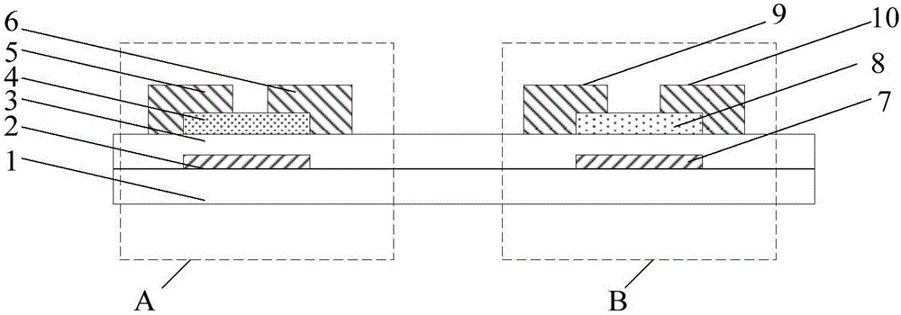
[0073] This embodiment provides a method for manufacturing an array substrate, the array substrate includes a display region and a GOA region, and the method includes:

[0074] making the active layer of the first thin film transistor in the display area by using a metal oxide semiconductor material;

[0075] The active layer of the second thin film transistor in the GOA region is fabricated by using non-metal oxide semiconductor material.

[0076] In this embodiment, the active layer of the thin film transistor in the display area of ​​the array substrate and the active layer of the thin film transistor in the GOA area are made of different materials, and the active layer of the thin film transistor in the display area of ​​the array substrate is made of metal oxide In this way, when the resolution of display products is very high, due to the relatively high mobility of metal oxide semiconductor materials, it can also meet the charging rate requirements of high-resolution dis...

Embodiment 2

[0109] Taking the fabrication of a bottom-gate array substrate as an example, the fabrication method of the array substrate of the present invention will be further introduced in conjunction with the accompanying drawings:

[0110] The manufacturing method of the array substrate in this embodiment specifically includes the following steps:

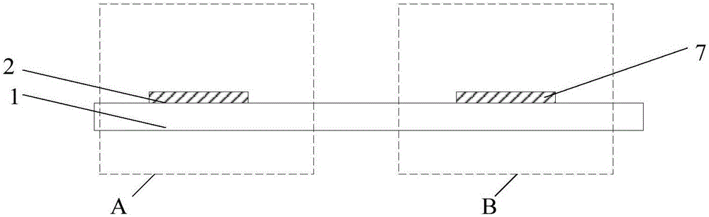
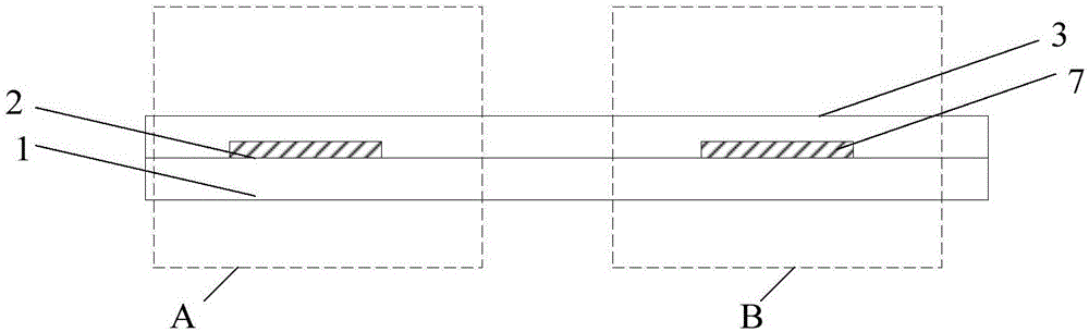
[0111] Step 1, such as figure 2 As shown, a base substrate 1 is provided, and the gate electrode 2 of the thin film transistor in the display area, the gate electrode 7 and the gate line pattern of the thin film transistor in the GOA area are formed on the base substrate 1;

[0112] Wherein, the base substrate may be a glass substrate or a quartz substrate. Specifically, sputtering or thermal evaporation can be used to deposit a thickness of about The gate metal layer, the gate metal layer can be Cu, Al, Ag, Mo, Cr, Nd, Ni, Mn, Ti, Ta, W and other metals and alloys of these metals, the gate metal layer can be single-layer structure or ...

Embodiment 3

[0123] Taking the fabrication of a bottom-gate array substrate as an example, the fabrication method of the array substrate of the present invention will be further introduced in conjunction with the accompanying drawings:

[0124] The manufacturing method of the array substrate in this embodiment specifically includes the following steps:

[0125] Step 1, such as figure 2 As shown, a base substrate 1 is provided, and the gate electrode 2 of the thin film transistor in the display area, the gate electrode 7 and the gate line pattern of the thin film transistor in the GOA area are formed on the base substrate 1;

[0126] Wherein, the base substrate may be a glass substrate or a quartz substrate. Specifically, sputtering or thermal evaporation can be used to deposit a thickness of about The gate metal layer, the gate metal layer can be Cu, Al, Ag, Mo, Cr, Nd, Ni, Mn, Ti, Ta, W and other metals and alloys of these metals, the gate metal layer can be single-layer structure or ...


PUM


Abstract

The invention provides an array substrate, a manufacturing method thereof and a display device, and belongs to the technical field of display. The array substrate comprises a display area and a GOA (Gate Driver on Array) area. The manufacturing method comprises the following steps: making an active layer of a first thin film transistor in the display area by a metallic oxide semiconductor material; making an active layer of a second thin film transistor of the GOA area by a non-metallic oxide semiconductor material. Through the technical scheme, a GOA technology can be applied to a high-resolution display device.

Description

technical field [0001] The present invention relates to the field of display technology, in particular to an array substrate, a manufacturing method thereof, and a display device. Background technique [0002] At present, with the development of display technology, in order to enhance product competitiveness, the resolution of display products is getting higher and higher, and the resolution of display products can reach 4K, or even 8K; at the same time, in order to save the cost of display products, GOA (Gate Driver Array) technology has been widely used. GOA technology is array substrate row driving technology. It uses thin film transistor (Thin Film Transistor) process to manufacture gate scanning driving circuit on thin film transistor array substrate to realize progressive scanning. , has the advantages of reducing the production cost and realizing the narrow bezel design of the panel, and is used for various display products. [0003] Due to the high resolution of dis...

Claims


Application Information

Patent Timeline
Patent Type & Authority Applications(China)
IPC IPC(8): H01L27/12H01L21/77
CPCH01L21/77H01L27/1214H01L27/1259H01L2021/775H01L29/24H01L29/66969H01L27/1225H01L29/42364H01L29/7869H01L29/66765H01L27/127H01L27/1262H01L29/78669H01L29/78678H01L27/1229H01L27/124H01L29/42384H01L29/4908H01L21/0274H01L21/02274H01L21/02565H01L27/1288H01L29/42372
Inventor 王谦
Owner BOE TECH GRP CO LTD
Why Eureka
Try Eureka