Electronic whiteboard equipment automatic pixel mapping method

An electronic whiteboard and pixel mapping technology, applied in the direction of electronic digital data processing, instruments, data processing input/output process, etc., can solve the problems of collection errors, interference spot 5, positioning spot 8 and insufficient light sensitivity, and improve accuracy , Improve the effect of collection quality

Inactive Publication Date: 2013-03-27
NANJING MAGON OPTO ELECTRICAL SCI & TECH
View PDF4 Cites 7 Cited by
  • Summary
  • Abstract
  • Description
  • Claims
  • Application Information

AI Technical Summary

Problems solved by technology

However, when the electronic whiteboard device 3 is used to actively align the positioning spot 8, since the positioning spot 8 itself is visible light, the acquisition of the positioning spot 8 through a filter will cause insufficient light sensitivity, resulting in acquisition errors, and making projection-camera mapping correction impossible.
[0007] In view of the problem that the positioning light spot 8 is insufficiently sensitive when the electronic whiteboard device 3 actively locates the positioning spot 8, a dual-band filter is generally used to replace the filter originally set on the optical path of the electronic whiteboard device 3. The dual-band filter can A part of visible light is reserved to ensure the sensitivity of spot 8 during automatic pixel mapping; however, the dual-band filter enhances the light transmission of visible light, and the visible light other than the infrared stylus will be collected by the electronic whiteboard device 3 during normal use, resulting in no Misoperation or interference occurs when the infrared stylus is operated. For this reason, it is necessary to add a circuit and increase the computing time to eliminate the interference light.
[0008] In addition if Figure 4 As shown, during automatic pixel mapping, in addition to the positioning spot 8 on the camera plane P3, there may also be an interference spot 5, the electronic whiteboard device 3 collects the image of the entire camera plane P3, and the positioning spot 8 and the interference spot 5 information is collected into the processor for calculation at the same time, calculation errors will inevitably occur, making the one-to-one mapping relationship between the projection plane P2 and the camera plane P3 wrong
[0009] Furthermore, during automatic pixel mapping, the electronic whiteboard device 3 collects and calculates the images of the entire imaging plane P3, which requires a large memory capacity, which increases the cost and volume of the entire device.
[0010] At the same time, due to the different use environments, the installation position of the electronic whiteboard device 3 in conjunction with the projector 2 relative to the projection screen 4 is also different. In terms of general installation habits, there are two ways to install the electronic whiteboard device 3. One is formal installation. , the other is reverse installation: if the electronic whiteboard device 3 is installed in a front-mounted manner, the viewing angles of the images displayed on the projection plane P2 and the camera plane P3 are consistent, and there may be a slight deviation due to installation deviations; if the electronic whiteboard device 3 is installed in a reverse Installation method, the angle of view of the screen displayed on the projection plane P2 and the camera plane P3 has a 180° flip, and there may be a slight deviation due to the deviation of the installation
In order to accurately obtain the one-to-one mapping relationship between the projection plane P2 and the camera plane P3, it is necessary to manually select the installation method of the electronic whiteboard device 3, otherwise it will be difficult to determine the projection plane P2 and the camera plane P3 according to the expected target. One-to-one mapping relationship, and currently there is no method that can automatically identify the installation method of the electronic whiteboard device 3

Method used


Image

  • Electronic whiteboard equipment automatic pixel mapping method
  • Electronic whiteboard equipment automatic pixel mapping method
  • Electronic whiteboard equipment automatic pixel mapping method

Examples


Embodiment Construction

[0030] The present invention will be further described below in conjunction with the accompanying drawings.

[0031] An automatic pixel mapping method for an electronic whiteboard device, comprising the following steps:

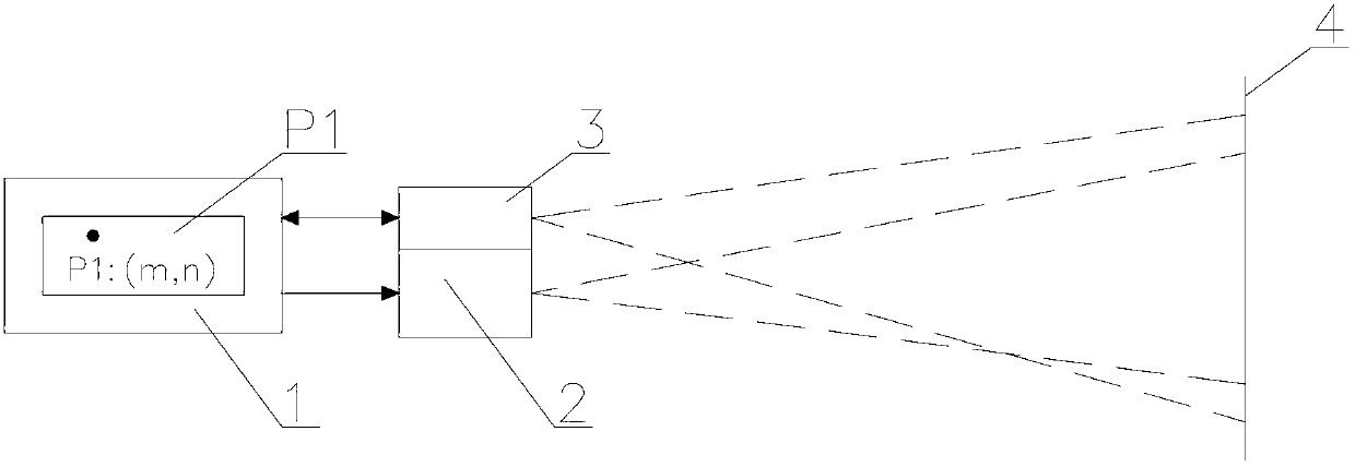
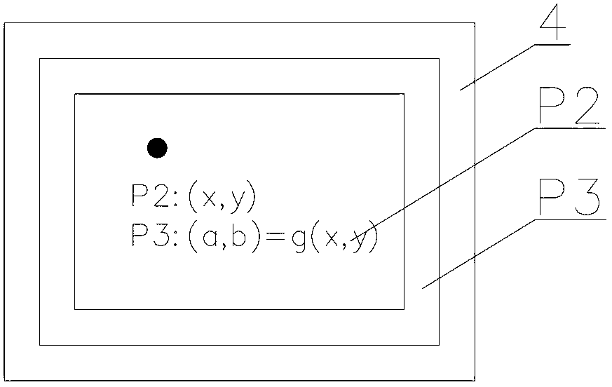
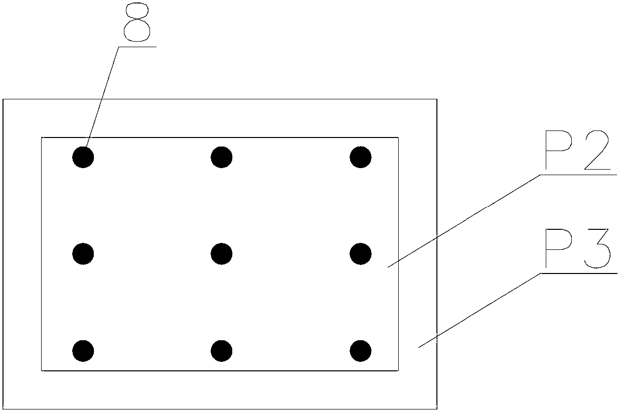
[0032] (1) if Figure 5 As shown, the camera plane P3 is divided into m units 6 by a rectangular grid with a unit length of n=3 pixels, each unit 6 includes n×n=3×3=9 pixel points 7, and the number of cycles k= 1;

[0033] (2) Projecting a number of positioning light spots 8 on the projection plane P2 and the camera plane P3;

[0034] (3) Position and collect the image of the camera plane P3 on the j=kth pixel of all m units, collect the grayscale / brightness value of the positioning spot on the m pixel point, and set the grayscale / brightness value to Calculate the center of gravity value G of the positioning spot image on the pixel point of the value ij , store the center of gravity value;

[0035] (4) k=k+1, judge whether k≤n×n is true, if the judgment ...


PUM


Abstract

The invention discloses an electronic whiteboard equipment automatic pixel mapping method. When collecting the information of a positioned light spot on an image pickup plane, the image information on the image pickup plane is continuously collected twice, wherein the projection of a positioned light spot exists during the first collection, and the image collected in the first collection is recorded as B; in the second collection, the projection of the positioned light spot does not exist, and the image collected in the second collection is recorded as A; and then, the information of the positioned light spot is obtained through a formula C=B-A. The electronic whiteboard equipment automatic pixel mapping method provided by the invention collects the information of the positioned light spot by an image subtraction method and can avoid the participation of an interference light spot into calculation; and meanwhile, the collection quality of the positioned light spot can be improved through the setting of a filter, and the projection-image pickup mapping accuracy is improved.

Description

technical field [0001] The invention relates to an electronic whiteboard device, in particular to an automatic pixel mapping method for the electronic whiteboard device. Background technique [0002] Such as figure 1 , figure 2 As shown, the electronic whiteboard device 3 is a paperless office device used in conjunction with the projector 2 , the projection screen 4 , the infrared stylus, and the PC 1 . During installation, the electronic whiteboard device 3 is installed with the projector 2 relative to the projection screen 4, the projector 2 will form a projection plane P2 on the projection screen 4, the electronic whiteboard device 3 will form a camera plane P3 on the projection screen 4, and the camera plane P3 Completely cover the projection plane P2; when in use, the PC 1 projects the screen information to be displayed through the projector 2 (for the convenience of description, the screen information to be displayed in the PC 1 is referred to as the display screen ...

Claims


Application Information

Patent Timeline
Patent Type & Authority Applications(China)
IPC IPC(8): G06F3/042
Inventor 戚海峰
Owner NANJING MAGON OPTO ELECTRICAL SCI & TECH
Why Eureka
Try Eureka